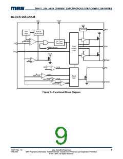
NB671, 24V, HIGH CURRENT SYNCHRONOUS STEP-DOWN CONVERTER
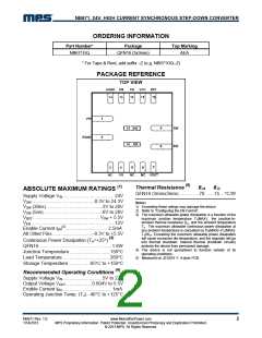
ORDERING INFORMATION
Part Number*
Package
Top Marking
NB671GQ
QFN16 (3x3mm)
AEA
* For Tape & Reel, add suffix –Z (e.g. NB671GQ–Z)
PACKAGE REFERENCE
TOP VIEW
Thermal Resistance (5)
QFN16 (3mmx3mm) ...............70 ...... 15...°C/W
θJA
θJC
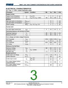
ABSOLUTE MAXIMUM RATINGS (1)
Supply Voltage VIN ....................................... 24V
V
V
V
SW...............................................-0.3V to 24.3V
SW (30ns)..........................................-3V to 28V
SW (5ns)............................................-6V to 28V
Notes:
1) Exceeding these ratings may damage the device.
2) Refer to “Configuring the EN Control”.
3) The maximum allowable power dissipation is a function of the
maximum junction temperature TJ(MAX), the junction-to-
ambient thermal resistance θJA, and the ambient temperature
TA. The maximum allowable continuous power dissipation at
any ambient temperature is calculated by PD(MAX)=(TJ(MAX)-
TA)/θJA. Exceeding the maximum allowable power dissipation
will cause excessive die temperature, and the regulator will go
into thermal shutdown. Internal thermal shutdown circuitry
protects the device from permanent damage.
VBST ................................................... VSW + 5.5V
V
EN ............................................................... 12V
Enable Current IEN(2)................................ 2.5mA
All Other Pins..............................–0.3V to +5.5V
(3)
Continuous Power Dissipation (TA=+25°)
QFN16...……………………….…..…………1.8W
Junction Temperature...............................150°C
Lead Temperature ....................................260°C
Storage Temperature............... -65°C to +150°C
4) The device is not guaranteed to function outside of its
operating conditions.
5) Measured on JESD51-7, 4-layer PCB.
Recommended Operating Conditions (4)
Supply Voltage VIN ..............................5V to 22V
Output Voltage VOUT....................0.604V to 5.5V
Enable Current IEN...................................... 1mA
Operating Junction Temp. (TJ). -40°C to +125°C
NB671 Rev. 1.0
1/14/2013
www.MonolithicPower.com
MPS Proprietary Information. Patent Protected. Unauthorized Photocopy and Duplication Prohibited.
© 2013 MPS. All Rights Reserved.
2

 MPS [ MONOLITHIC POWER SYSTEMS ]