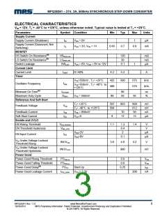
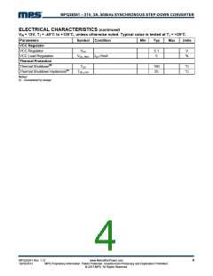
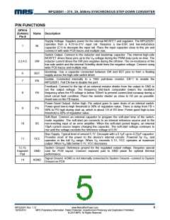
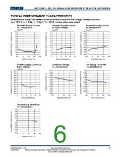
MPQ28261 – 21V, 3A, 500kHz SYNCHRONOUS STEP-DOWN CONVERTER
PIN FUNCTIONS
QFN14
(3x4mm)
Pin #
Name Description
Supply Voltage. Supplies power for the internal MOSFET and regulator. The MPQ28261
operates from a 4.5V-to-21V input rail. Requires a low-ESR and low-inductance
capacitor (C1) to decouple the input rail. Place the input capacitor close to this pin and
connect it with wide PCB traces and multiple vias.
1
IN
Switch Output. Connect to the inductor and bootstrap capacitor. The internal high-side
MOSFET drives these pins up to the VIN voltage during the PWM duty-cycle on-time. The
inductor current drives the SW pins negative during the off-time. The on-resistance of the
low-side switch and the internal Schottky diode fixes the negative voltage. Connect using
wide PCB traces and multiple vias.
2,3,4,5
SW
Bootstrap. Use a capacitor connected between SW and BST pins to form a floating
supply across the high-side switch driver.
6
7
BST
EN
Enable. Connected internally to a 1Mꢀ pull-down resistor. EN=1 to enable the
MPQ28261. Pull EN low to disable the part.
Feedback. Connect to the tap of an external resistor divider from the output to GND to
set the output voltage. The frequency fold-back comparator lowers the oscillator
frequency when the FB voltage is below 100mV to prevent current-limit runaway during a
short circuit fault condition. Place the resistor divider as close to FB pin as possible.
Avoid vias on the FB traces.
8
9
FB
PG
Power-Good Output. Active high. Pin output goes to open drain of an internal switch.
Power-good low-to-high threshold is 90% of regulation value. There is delay from FB ≥
90% to PG high during start up, which is about 1/4 of SS time. Power-good high-to-low
threshold is 80% of regulation value.
Soft-Start. Connect an external capacitor to program the soft-start time of the switch-
mode regulator. The soft-start pin connects to an internal reference source and to the
non-inverting input of an error amplifier. When the soft-start period begins, an internal
10µA current source begins charging the capacitor. The soft-start voltage continues to
rise until the voltage exceeds the reference voltage of 0.6V.
10
11
SS
Bias Supply. Typical level of around 5.1V. Decouple with a 0.1μF-up-to-0.22μF capacitor.
Provides most of the power to the device’s internal circuits. Powered by VIN, and
operates in the full VIN range. When VIN exceeds 5.1V, VCC operates at maximum
output. When VIN falls below 5.1V, VCC decreases.
VCC
12,13,
Exposed
Pad
System Ground. Reference ground for the regulated output voltage. Requires special
care for PCB layout. Connect exposed pad to GND plane for optimal thermal
performance.
GND
Signal Ground. AGND is not internally connected to System Ground—connect to System
Ground on PCB.
14
AGND
MPQ28261 Rev. 1.12
10/10/2013
www.MonolithicPower.com
MPS Proprietary Information. Patent Protected. Unauthorized Photocopy and Duplication Prohibited.
© 2013 MPS. All Rights Reserved.
5

 MPS [ MONOLITHIC POWER SYSTEMS ]