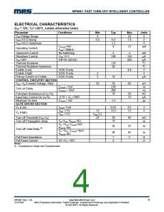
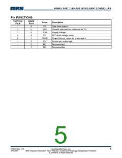
MP6901- FAST TURN-OFF INTELLIGENT CONTROLLER
function after the junction temperature has
synchronous MOSFET to ease the rise of Vds.
By doing that, Vds is adjusted to be around -
70mV even when the current through the MOS is
fairly small, this function can make the driver
voltage fairly low when the synchronous
MOSFET is turned off to fast the turn off speed
(this function is still active during turn on blanking
time which means the gate driver could still be
turned off even with very small duty of the
synchronous MOSFET).
dropped to 120oC.
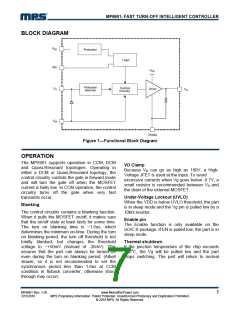
Thermal Design
If the dissipation of the chip is higher than
100mW due to switching frequencies above
100kHz, VDD higher than 15V and/or Cload
larger than 5nF, it is recommended to use the
thermally-enhanced SOIC-8.
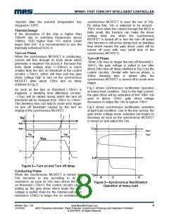
Turn-on Phase
When the synchronous MOSFET is conducting,
current will flow through its body diode which
generates a negative Vds across it. Because this
body diode voltage drop (<-500mV) is much
smaller than the turn on threshold of the control
circuitry (-70mV), which will then pull the gate
driver voltage high to turn on the synchronous
MOSFET after about 150ns turn on delay
(Defined in Fig.2).
Turn-off Phase
When Vds rises to trigger the turn off threshold (-
30mV), the gate voltage is pulled to low after
about 20ns turn off delay (defined in Fig.2) by the
control circuitry. Similar with turn-on phase, a
200ns blanking time is added after the
synchronous MOSFET is turned off to avoid error
trigger.
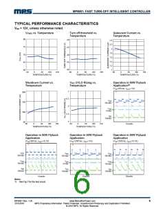
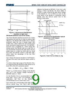
Fig.3 shows synchronous rectification operation
at heavy load condition. Due to the high current,
the gate driver will be saturated at first. After Vds
goes to above -70mV, gate driver voltage
decreases to adjust the Vds to typical -70mV.
As soon as the turn on threshold (-70mV) is
triggered, a blanking time (Minimum on-time:
~1.6us) will be added during which the turn off
threshold will be changed from -30mV to +50mV.
This blanking time can help to avoid error trigger
on turn off threshold caused by the turn on
ringing of the synchronous MOSFET.
Fig.4 shows synchronous rectification operation
at light load condition. Due to the low current, the
gate driver voltage never saturates but begins to
decrease as soon as the synchronous MOSFET
is turned on and adjust the Vds.
V
DS
-30mV
-70mV
Vds
-30mV
tDon
tDoff
-70mV
V
GATE
2V
Isd
Figure 2—Turn on and Turn off delay
Conducting Phase
When the synchronous MOSFET is turned on,
Vds becomes to rise according to its on
resistance, as soon as Vds rises above the turn
on threshold (-70mV), the control circuitry stops
pulling up the gate driver which leads the gate
voltage is pulled down by the internal pull-down
resistance (10kΩ) to larger the on resistance of
Vgs
t0
t1
t2
Figure 3—Synchronous Rectification
Operation at heavy load
MP6901 Rev. 1.05
3/15/2016
www.MonolithicPower.com
MPS Proprietary Information. Patent Protected. Unauthorized Photocopy and Duplication Prohibited.
© 2016 MPS. All Rights Reserved.
8

 MPS [ MONOLITHIC POWER SYSTEMS ]