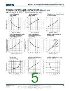
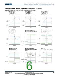
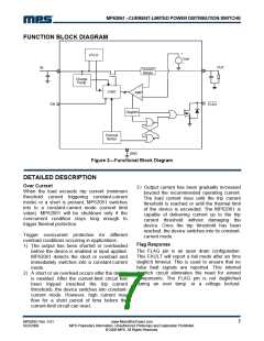
MP62061 –CURRENT-LIMITED POWER DISTRIBUTION SWITCHE
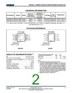
ORDERING INFORMATION
Maximum
Short-Circuit
Current
Maximum
Switch Continuous
Load Current
Top
Marking
Temperature
Part Number* Enable
Package
@ TA=25°C
MP62061DH Active High Single
MP62061DN Active High Single
700mA
700mA
1250mA
1250mA
MSOP8E 62061D
SOIC8E 62061D
–40°C to +85°C
–40°C to +85°C
*For Tape & Reel, add suffix –Z (eg. MP62061DH–Z); For RoHS Compliant Packaging, add suffix –LF ;
(eg. MP62061DH–LF–Z)
PACKAGE REFERENCE
TOP VIEW
TOP VIEW
GND
IN
1
2
3
4
8
7
6
5
OUT
OUT
OUT
FLAG
GND
IN
OUT
OUT
OUT
FLAG
1
2
3
4
8
7
6
5
IN
IN
EN
EN
EXPOSED PAD
ON BACKSIDE
CONNECT TO GND
EXPOSED PAD
ON BACKSIDE
CONNECT TO GND
MSOP8E
SOIC8E
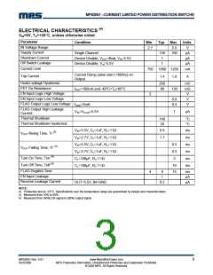
ABSOLUTE MAXIMUM RATINGS (1)
Thermal Resistance (3)
θJA
θJC
IN .................................................-0.3V to +6.0V
EN, FLAG, OUT to GND..............-0.3V to +6.0V
Continuous Power Dissipation (TA = +25°C) (2)
MSOP8E.................................................... 2.3W
SOIC8E...................................................... 2.5W
Junction Temperature...............................150°C
Lead Temperature ....................................260°C
Storage Temperature...............–65°C to +150°C
Operating Temperature..............–40°C to +85°C
MSOP8E.................................55...... 12... °C/W
SOIC8E ..................................50...... 10... °C/W
Notes:
1) Exceeding these ratings may damage the device.
2) The maximum allowable power dissipation is a function of the
maximum junction temperature TJ(MAX), the junction-to-
ambient thermal resistance θJA, and the ambient temperature
TA. The maximum allowable continuous power dissipation at
any ambient temperature is calculated by PD(MAX)=(TJ(MAX)-
TA)/θJA. Exceeding the maximum allowable power dissipation
will cause excessive die temperature, and the regulator will go
into thermal shutdown. Internal thermal shutdown circuitry
protects the device from permanent damage.
3) Measured on JESD51-7 4-layer PCB
MP62061 Rev. 0.91
9/23/2009
www.MonolithicPower.com
MPS Proprietary Information. Unauthorized Photocopy and Duplication Prohibited.
© 2009 MPS. All Rights Reserved.
2

 MPS [ MONOLITHIC POWER SYSTEMS ]