MP4462 – 3.5A, 4MHz, 36V STEP-DOWN CONVERTER
High Frequency Operation
The switching frequency of MP4462 can be
Layout becomes more important when the
device switches at higher frequency. It is
programmed up to 4MHz by an external resistor.
Please pay attention to the following if the
switching frequency is above 2MHz.
essential to place the input decoupling
capacitor, catch diode and the MP4462 (Vin pin,
SW pin and PGND) as close as possible, with
traces that are very short and fairly wide. This
can help to greatly reduce the voltage spike on
SW node, and lower the EMI noise level as well.
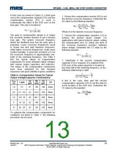
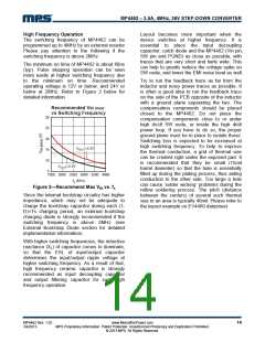
The minimum on time of MP4462 is about 80ns
(typ). Pulse skipping operation can be seen
more easily at higher switching frequency due
to the minimum on time. Recommended
operating voltage is 12V or below, and 24V or
below at 2MHz. Refer to Figure 2 below for
detailed information.
Try to run the feedback trace as far from the
inductor and noisy power traces as possible. It
is often a good idea to run the feedback trace
on the side of the PCB opposite of the inductor
with a ground plane separating the two. The
compensation components should be placed
closed to the MP4462. Do not place the
compensation components close to or under
high dv/dt SW node, or inside the high di/dt
power loop. If you have to do so, the proper
ground plane must be in place to isolate those.
Switching loss is expected to be increased at
high switching frequency. To help to improve
the thermal conduction, a grid of thermal vias
can be created right under the exposed pad. It
is recommended that they be small (15mil
barrel diameter) so that the hole is essentially
filled up during the plating process, thus aiding
conduction to the other side. Too large a hole
can cause ‘solder wicking’ problems during the
reflow soldering process. The pitch (distance
between the centers) of several such thermal
vias in an area is typically 40mil. Please refer to
the layout example on EV4460 datasheet.
Recommended VIN (max)
vs Switching Frequency
30
25
20
V
=3.3V
OUT
15
10
5
V
=2.5V
OUT
1500 2000 2500 3000 3500 4000
f (KHz)
s
Figure 2—Recommend Max VIN vs. fs
Since the internal bootstrap circuitry has higher
impedance, which may not be adequate to
charge the bootstrap capacitor during each (1-
D)×Ts charging period, an external bootstrap
charging diode is strongly recommended if the
switching frequency is above 2MHz (see
External Bootstrap Diode section for detailed
implementation information).
With higher switching frequencies, the inductive
reactance (XL) of capacitor comes to dominate,
so that the ESL of input/output capacitor
determines the input/output ripple voltage at
higher switching frequency. As a result of that,
high frequency ceramic capacitor is strongly
recommended as input decoupling capacitor
and output filtering capacitor for such high
frequency operation.
MP4462 Rev. 1.02
3/4/2013
www.MonolithicPower.com
MPS Proprietary Information. Patent Protected. Unauthorized Photocopy and Duplication Prohibited.
© 2013 MPS. All Rights Reserved.
14

 MPS [ MONOLITHIC POWER SYSTEMS ]