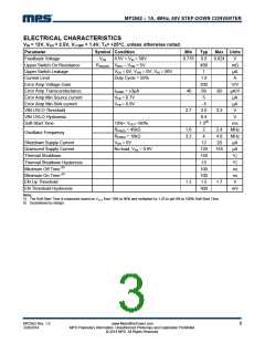
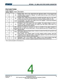
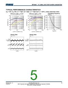
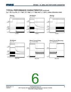
MP2562 – 1A, 4MHz, 50V STEP-DOWN CONVERTER
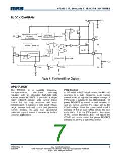
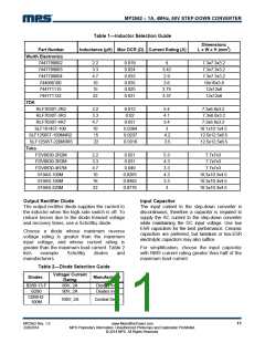
BLOCK DIAGRAM
V
VIN
IN
+
--
+
--
5V
2.6V
REFERENCE UVLO/
INTERNAL
REGULATORS
EN
THERMAL
SHUTDOWN
BST
SW
SW
--
+
I
SW
SS time
SS
V
OUT
I
Level
Shift
SW
FB
Gm Error Amp
--
+
COMP
SS
0V8
OSCILLATOR
CLK
V
OUT
FREQ
GND
COMP
Figure 1—Functional Block Diagram
OPERATION
The MP2562 is
non-synchronous,
a
variable frequency,
PWM Control
step-down switching
At moderate to high output current, the MP2562
operates in a fixed frequency, peak current
control mode to regulate the output voltage. A
PWM cycle is initiated by the internal clock. The
power MOSFET is turned on and remains on
until its current reaches the value set by the
COMP voltage. When the power switch is off, it
remains off for at least 100ns before the next
cycle starts. If, in one PWM period, the current
in the power MOSFET does not reach the
COMP set current value, the power MOSFET
remains on, saving a turn-off operation.
regulator with an integrated high-side high
voltage power MOSFET. It provides a single
highly efficient solution with current mode
control for fast loop response and easy
compensation. It features a wide input voltage
range, internal soft-start control and precision
current limiting. Its very low operational
quiescent current makes it suitable for battery
powered applications.
MP2562 Rev. 1.0
2/28/2014
www.MonolithicPower.com
MPS Proprietary Information. Unauthorized Photocopy and Duplication Prohibited.
© 2014 MPS. All Rights Reserved.
7

 MPS [ MONOLITHIC POWER SYSTEMS ]