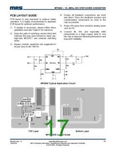
MP2562 – 1A, 4MHz, 50V STEP-DOWN CONVERTER
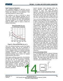
In this case (as shown in TYPICAL
APPLICATION), a third pole set by the
compensation capacitor (C6) and the
compensation resistor (R3) is used to
compensate the effect of the ESR zero on the
loop gain. This pole is located at:
1. Choose the compensation resistor (R3) to set
the desired crossover frequency. Determine the
R3 value by the following equation:
2 C2 fC VOUT
R3
GEA GCS
VFB
1
Where fC is the desired crossover frequency.
fP3
2 C6 R3
2. Choose the compensation capacitor (C3) to
achieve the desired phase margin. For
applications with typical inductor values, setting
the compensation zero, fZ1, below one forth of
the crossover frequency provides sufficient
phase margin. Determine the C3 value by the
following equation:
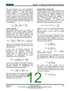
The goal of compensation design is to shape
the converter transfer function to get a desired
loop gain. The system crossover frequency
where the feedback loop has the unity gain is
important. Lower crossover frequencies result
in slower line and load transient responses,
while higher crossover frequencies could cause
system unstable. A good rule of thumb is to set
the crossover frequency to approximately one-
tenth of the switching frequency. The Table 3
lists the typical values of compensation
components for some standard output voltages
with various output capacitors and inductors.
The values of the compensation components
have been optimized for fast transient
responses and good stability at given conditions.
4
C3
2 R3 fC
3. Determine if the second compensation
capacitor (C6) is required. It is required if the
ESR zero of the output capacitor is located at
less than half of the switching frequency, or the
following relationship is valid:
fS
2
1
2 C2 RESR
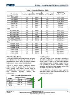
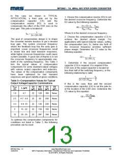
Table 3—Compensation Values for Typical
Output Voltage/Capacitor Combinations
If this is the case, then add the second
compensation capacitor (C6) to set the pole fP3
at the location of the ESR zero. Determine the
C6 value by the equation:
VOUT
(V)
C2
(µF)
R3
(kꢀ)
C3
(pF)
C6
(pF)
L (µH)
4.7
1.8
2.5
3.3
5
22
22
22
22
22
120
82
100
330
220
150
150
None
None
None
None
None
C2 RESR
C6
R3
4.7 - 6.8
6.8 -10
15 - 22
22 - 33
120
158
287
12
To optimize the compensation components for
conditions not listed in Table 3, the following
procedure can be used.
MP2562 Rev. 1.0
2/28/2014
www.MonolithicPower.com
MPS Proprietary Information. Unauthorized Photocopy and Duplication Prohibited.
© 2014 MPS. All Rights Reserved.
13

 MPS [ MONOLITHIC POWER SYSTEMS ]