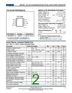
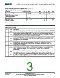
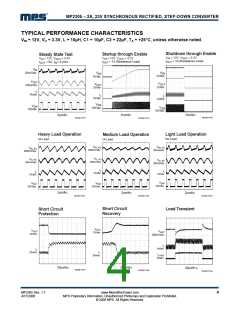
TM
MP2305 – 2A, 23V SYNCHRONOUS RECTIFIED, STEP-DOWN CONVERTER
In this case (as shown in Figure 2), a third pole
set by the compensation capacitor (C6) and the
compensation resistor (R3) is used to
compensate the effect of the ESR zero on the
loop gain. This pole is located at:
3. Determine if the second compensation
capacitor (C6) is required. It is required if the
ESR zero of the output capacitor is located at
less than half of the switching frequency, or the
following relationship is valid:
fS
2
1
1
fP3
=
<
2π× C6×R3
2π × C2× RESR
The goal of compensation design is to shape
the converter transfer function to get a desired
loop gain. The system crossover frequency
where the feedback loop has the unity gain is
important. Lower crossover frequencies result
in slower line and load transient responses,
while higher crossover frequencies could cause
system instability. A good rule of thumb is to set
the crossover frequency below one-tenth of the
switching frequency.
If this is the case, then add the second
compensation capacitor (C6) to set the pole fP3
at the location of the ESR zero. Determine the
C6 value by the equation:
C2 × RESR
C6 =
R3
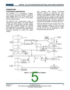
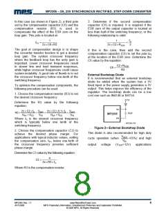
External Bootstrap Diode
It is recommended that an external bootstrap
diode be added when the system has a 5V
fixed input or the power supply generates a 5V
output. This helps improve the efficiency of the
regulator. The bootstrap diode can be a low
cost one such as IN4148 or BAT54.
To optimize the compensation components, the
following procedure can be used.
1. Choose the compensation resistor (R3) to set
the desired crossover frequency.
5V
Determine the R3 value by the following
equation:
BS
2π × C2 × fC VOUT 2π × C2 × 0.1× fS VOUT
R3 =
×
<
×
10nF
MP2305
GEA × GCS
VFB
GEA × GCS
VFB
SW
Where fC is the desired crossover frequency
which is typically below one tenth of the
switching frequency.
MP2305_F02
Figure 2—External Bootstrap Diode
2. Choose the compensation capacitor (C3) to
achieve the desired phase margin. For
applications with typical inductor values, setting
the compensation zero, fZ1, below one-forth of
the crossover frequency provides sufficient
phase margin.
This diode is also recommended for high duty
VOUT
cycle operation (when
>65%) and high
VIN
(VOUT>12V)
output
voltage
applications
Determine the C3 value by the following equation:
4
C3 >
2π × R3 × fC
Where R3 is the compensation resistor.
MP2305 Rev. 1.7
4/17/2006
www.MonolithicPower.com
MPS Proprietary Information. Unauthorized Photocopy and Duplication Prohibited.
© 2006 MPS. All Rights Reserved.
8

 MPS [ MONOLITHIC POWER SYSTEMS ]