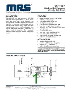
MP1907―100V, 2.5A, HIGH FREQUENCY HALF-BRIDGE GATE DRIVER
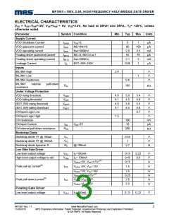
ELECTRICAL CHARACTERISTICS (continued)
VDD = VBST-VSW=12V, VSS=VSW = 0V, VEN=3.3V, No load at DRVH and DRVL, TA= +25°C, unless
otherwise noted.
Parameter
Symbol Condition
Min
Typ
0.45
0.25
1.5
Max
Units
High level output voltage to rail
VOHH
IO=-100mA
0.6
V
A
A
A
A
VDRVH=0V , VBST - VSW =5V (8)
VDRVH=0V, VDD=12V
VDRVH=0V, VDD=16V
VDRVH=VBST - VSW =5V (8)
Peak pull-up current(6)
IOHH
2.5
0.65
Peak pull-down current(6)
IOLH
VDRVH=VDD=12V
VDRVH=VDD=16V
2.5
3.5
A
A
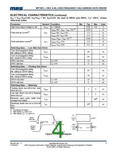
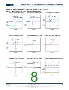
Switching Spec. --- Low Side Gate Driver
Turn-off propagation delay
TDLFF
20
20
ns
ns
INL falling to DRVL falling
Turn-on propagation delay
TDLRR
INL rising to DRVL rising
DRVL rise time
CL=1nF
CL=1nF
12
9
ns
ns
DRVL fall time
Switching Spec. --- Floating Gate Driver
Turn-off propagation delay
TDHFF
20
18
ns
ns
INL falling to DRVH falling
Turn-on propagation delay
TDHRR
INL rising to DRVH rising
DRVH rise time
CL=1nF
CL=1nF
12
9
ns
ns
DRVH fall time
Switching Spec. --- Matching
Floating driver turn-off to low side
drive turn-on
TMON
1
1
5
5
ns
ns
ns
ns
Low side driver turn-off to floating
driver turn-on
TMOFF
Minimum input pulse width that
changes the output
TPW
50(6)
Bootstrap diode turn-on or turn-off
time
TBS
10(6)
Note:
6) Guaranteed by design.
7) After startup VDD fall to 4.5V
8) After startup VBST- VSW fall to 5V
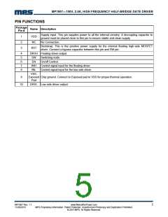
INL
INPUT
(INH, INL)
INH
T
DHRR, TDLRR
TDHFF, TDLFF
DRVL
OUTPUT
(DRVH,
DRVL)
TMON
TMOFF
DRVH
Figure 1—Timing Diagram
MP1907 Rev. 1.1
11/20/2013
www.MonolithicPower.com
MPS Proprietary Information. Patent Protected. Unauthorized Photocopy and Duplication Prohibited.
© 2013 MPS. All Rights Reserved.
4

 MPS [ MONOLITHIC POWER SYSTEMS ]