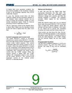
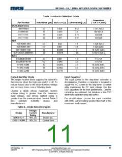
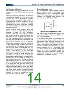
MP1584 – 3A, 1.5MHz, 28V STEP-DOWN CONVERTER
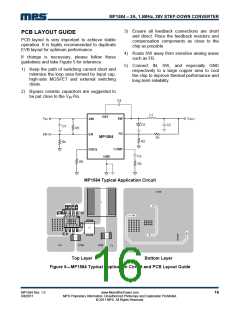
3) Ensure all feedback connections are short
and direct. Place the feedback resistors and
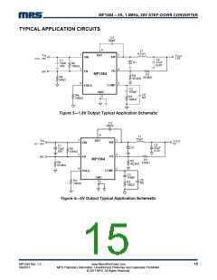
PCB LAYOUT GUIDE
PCB layout is very important to achieve stable
operation. It is highly recommended to duplicate
EVB layout for optimum performance.
compensation components as close to the
chip as possible.
4) Route SW away from sensitive analog areas
such as FB.
If change is necessary, please follow these
guidelines and take Figure 5 for reference.
5) Connect IN, SW, and especially GND
respectively to a large copper area to cool
the chip to improve thermal performance and
long-term reliability.
1) Keep the path of switching current short and
minimize the loop area formed by Input cap,
high-side MOSFET and external switching
diode.
2) Bypass ceramic capacitors are suggested to
be put close to the VIN Pin.
C4
L1
BST
V
V
OUT
SW
FB
IN
VIN
D1
R2
C2
C1
R4
R5
EN
EN
MP1584
R1
COMP
FREQ
C3
R3
GND
R6
MP1584 Typical Application Circuit
Top Layer
Bottom Layer
Figure 5―MP1584 Typical Application Circuit and PCB Layout Guide
MP1584 Rev. 1.0
8/8/2011
www.MonolithicPower.com
MPS Proprietary Information. Unauthorized Photocopy and Duplication Prohibited.
© 2011 MPS. All Rights Reserved.
16

 MPS [ MONOLITHIC POWER SYSTEMS ]