Bus Signal Timing
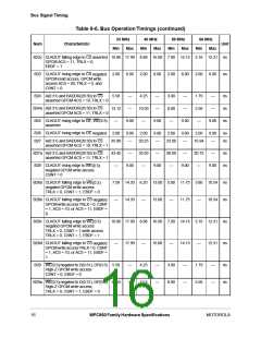
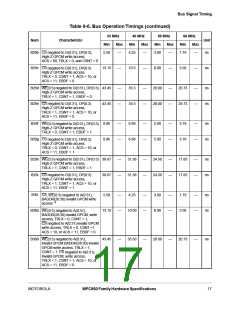
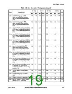
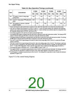
Table 9-6. Bus Operation Timings (continued)
33 MHz
40 MHz
50 MHz
66 MHz
Num
Characteristic
Unit
Min
7.00
Max
Min
Max
Min
Max
Min
Max
B41 TS valid to CLKOUT rising edge
(setup time)
—
7.00
2.00
—
—
7.00
2.00
—
—
7.00
2.00
—
—
ns
ns
ns
B42 CLKOUT rising edge toTS valid (hold 2.00
time)
—
—
—
—
B43 AS negation to memory controller
signals negation
—
TBD
TBD
TBD
TBD
1
2
Phase and frequency jitter performance results are only valid if the input jitter is less than the prescribed value.
If the rate of change of the frequency of EXTAL is slow (i.e., it does not jump between the minimum and maximum
values in one cycle) or the frequency of the jitter is fast (i.e., it does not stay at an extreme value for a long time) then
the maximum allowed jitter on EXTAL can be up to 2%.
3
4
The timings specified in B4 and B5 are based on full strength clock.
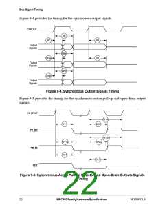
The timing for BR output is relevant when the MPC860 is selected to work with external bus arbiter.The timing for BG
output is relevant when the MPC860 is selected to work with internal bus arbiter.
5
6
7
The timing required for BR input is relevant when the MPC860 is selected to work with internal bus arbiter.The timing
for BG input is relevant when the MPC860 is selected to work with external bus arbiter.
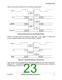
The D(0:31) and DP(0:3) input timings B18 and B19 refer to the rising edge of the CLKOUT in which the TA input
signal is asserted.
The D(0:31) and DP(0:3) input timings B20 and B21 refer to the falling edge of the CLKOUT.This timing is valid only
for read accesses controlled by chip-selects under control of the UPM in the memory controller, for data beats where
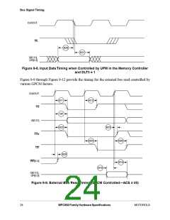
DLT3 = 1 in the UPM RAM words. (This is only the case where data is latched on the falling edge of CLKOUT.)
8
9
The timing B30 refers to CS when ACS = 00 and to WE(0:3) when CSNT = 0.
The signal UPWAIT is considered asynchronous to the CLKOUT and synchronized internally. The timings specified
in B37 and B38 are specified to enable the freeze of the UPM output signals as described in Figure 9-17.
10
The AS signal is considered asynchronous to the CLKOUT.The timing B39 is specified in order to allow the behavior
specified in Figure 9-20.
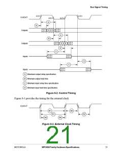
Figure 9-2 is the control timing diagram.
20
MPC860 Family Hardware Specifications
MOTOROLA

 MOTOROLA [ MOTOROLA ]