Freescale Semiconductor, Inc.
MSCAN Controller
Clock System
one bit time is generated. As the msCAN12 receiver engine also
receives the frames being sent by itself, a timer signal is also generated
after a successful transmission.
The previously described timer signal can be routed into the on-chip
timer interface module (ECT). This signal is connected to the Timer n
(1)
Channel m input under the control of the timer link enable (TLNKEN)
bit in the CMCR0.
After timer n has been programmed to capture rising edge events, it can
be used under software control to generate 16-bit time stamps which can
be stored with the received message.
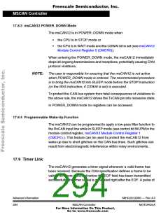
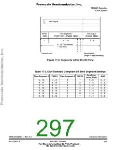
17.10 Clock System
Figure 17-7 shows the structure of the msCAN12 clock generation
circuitry. With this flexible clocking scheme the msCAN12 is able to
handle CAN bus rates ranging from 10 kbps up to 1 Mbps.
CGM
msCAN12
SYSCLK
EXTALi
Time quanta
clock
CGMCANCLK
Prescaler
(1...64)
CLKSRC
CLKSRC
Figure 17-7. Clocking Scheme
The clock source bit (CLKSRC) in the msCAN12 module control register
(CMCR1) (see msCAN12 Bus Timing Register 0 (CBTR0)) defines
whether the msCAN12 is connected to the output of the crystal oscillator
(EXTALi) or to a clock twice as fast as the system clock (ECLK).
The clock source has to be chosen such that the tight oscillator tolerance
requirements (up to 0.4%) of the CAN protocol are met. Additionally, for
high CAN bus rates (1 Mbps), a 50% duty cycle of the clock is required.
1. The timer channel being used for the timer link is integration dependent.
Advance Information
68HC(9)12D60 — Rev 4.0
MOTOROLA
MSCAN Controller
295
For More Information On This Product,
Go to: www.freescale.com

 MOTOROLA [ MOTOROLA ]