Freescale Semiconductor, Inc.
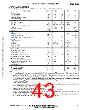
PCB Layout
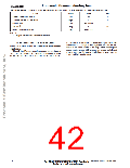
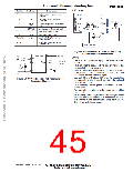
Pin No.
Pin Name
Description
1 thru 3
—
Redundant V . Leave uncon-
SS
STATUS
ST
P1
nected.
P0
4
5
ST
Logic input pin used to initiate
self–test.
V
SS
V
OUT
A/D IN
R
V
Output voltage of the accelerome-
ter.
OUT
C
0.1 µF
C
1 kΩ
0.01 µF
V
SS
V
DD
6
STATUS
Logic output pin to indicate fault.
The power supply ground.
The power supply input.
C
0.1 µF
V
DD
7
8
V
SS
V
RH
V
DD
C
0.1 µF
9 thru 13
Trim pins
Used for factory trim. Leave
unconnected.
14 thru 16
—
No internal connection. Leave
unconnected.
POWER SUPPLY
Figure 5. Recommend PCB Layout for Interfacing
Accelerometer to Microcontroller
6
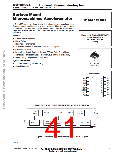
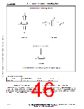
MMA1200D
STATUS
V
DD
NOTES:
LOGIC
INPUT
4
8
ST
R1
1 kΩ
•
•
•
Use a 0.1 µF capacitor on V
source.
to decouple the power
DD
5
OUTPUT
SIGNAL
V
V
OUT
DD
Physical coupling distance of the accelerometer to the
microcontroller should be minimal.
Place a ground plane beneath the accelerometer to reduce
noise, the ground plane should be attached to all of the
open ended terminals shown in Figure 4.
C1
0.1 µF
C2
0.01 µF
7
V
SS
•
Use an RC filter of 1 kΩ and 0.01 µF on the output of the
accelerometer to minimize clock noise (from the switched
capacitor filter circuit).
Figure 4. SOIC Accelerometer with Recommended
Connection Diagram
•
•
•
PCB layout of power and ground should not couple power
supply noise.
Accelerometer and microcontroller should not be a high
current path.
A/Dsamplingrateandanyexternalpowersupplyswitching
frequency should be selected such that they do not inter-
fere with the internal accelerometer sampling frequency.
This will prevent aliasing errors.
Motorola Sensor Device Data
www.motorola.com/semiconductors
Go to: www.freescale.com
2–9
For More Information On This Product,

 MOTOROLA [ MOTOROLA ]