MC12022LVA MC12022LVB
MAXIMUM RATINGS
Rating
Symbol
Value
Unit
Vdc
°C
Power Supply Voltage, Pin 2
Operating Temperature Range
Storage Temperature Range
Modulus Control Input, Pin 6
NOTE; ESD data available upon request.
V
CC
–0.5 to 7.0
–40 to 85
–65 to 150
–0.5 to 6.5
T
A
T
stg
°C
MC
Vdc
ELECTRICAL CHARACTERISTICS (V
= 4.5 to 5.5 V; T = –40°C to 85°C, unless otherwise noted.)
A
CC
Characteristic
Toggle Frequency (Sine Wave Input)
Symbol
Min
0.1
–
Typ
1.4
4.7
5.8
–
Max
1.1
6.5
8.0
Unit
GHz
mA
mA
V
f
t
Supply Current Output Unloaded (Pin 2)
Supply Current Output Unloaded (Pin 2) at 5.0 Vdc
Modulus Control Input High (MC)
I
CC
I
CCH
V
IH1
2.0
–
V
CC
Modulus Control Input Low (MC)
V
IL1
–
0.8
V
Divide Ratio Control Input High (SW)
Divide Ratio Control Input Low (SW)
V
V
V
V
Vdc
–
IH2
CC
CC
CC
V
Open
Open
Open
IL2
Output Voltage Swing (C = 12 pF; R = 1.1 kΩ at 2.7 Vdc)
V
0.8
1.0
–
1.0
1.6
11
–
–
V
V
L
L
out
pp
Output Voltage Swing (C = 12 pF; R = 2.2 kΩ at 5.0 Vdc)
V
out
L
L
pp
Modulus Setup Time MC to Out
t
16
ns
set
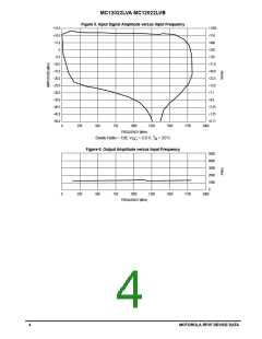
Input Voltage Sensitivity 250–1100 MHz
100–250 MHz
V
100
400
–
–
1500
1500
mVpp
in(min)
Output Current (C = 12 pF; R = 2.2 kΩ at 2.7 Vdc)
I
I
–
–
1.2
1.2
4.0
4.0
mA
mA
L
L
O
Output Current (C = 12 pF; R = 2.2 kΩ at 5.0 Vdc)
L
L
O
2
MOTOROLA RF/IF DEVICE DATA

 MOTOROLA [ MOTOROLA ]