V62C3801024L(L)
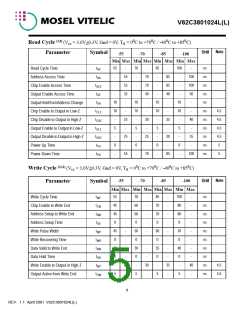
Read Cycle (3,9) (Vcc = 3.0V+0.3V, Gnd = 0V, TA = 00C to +700C / -400C to +850C)
Note
Unit
Parameter
Symbol
-55
-70
-85
-100
Min Max Min Max Min Max Min Max
tRC
tAA
tACE
tOE
55
-
-
70
-
-
85
-
-
100
-
100
100
50
-
ns
ns
ns
ns
ns
ns
ns
ns
ns
ns
ns
Read Cycle Time
55
55
35
-
70
70
40
-
85
85
40
-
-
-
Address Access Time
-
-
-
Chip Enable Access Time
Output Enable Access Time
OutputHold fromAddress Change
Chip Enable to Output in Low-Z
Chip Disable to Output in High-Z
Output Enable to Output in Low-Z
OutputDisable toOutput in High-Z
Power-Up Time
-
-
-
-
tOH
10
10
-
10
10
-
10
10
-
10
10
-
tCLZ
tCHZ
tOLZ
tOHZ
tPU
-
-
-
-
4,5
4,5
4,5
4,5
5
25
-
30
-
35
-
40
-
5
-
5
-
5
-
5
-
25
-
25
-
30
-
35
-
0
-
0
-
0
-
0
-
tPD
55
70
85
100
5
Power-Down Time
Write Cycle (3,11) (Vcc = 3.0V+0.3V, Gnd = 0V, TA = 00C to +700C / -400C to +850C)
Note
-55
-70
-85
-100
Unit
Parameter
Symbol
Min Max Min Max Min Max Min Max
tWC
tCW
tAW
tAS
55
45
45
0
-
-
70
60
60
0
-
-
85
70
70
0
-
-
100
80
80
0
-
-
ns
ns
ns
ns
ns
ns
ns
ns
ns
ns
Write Cycle Time
Chip Enable to Write End
Address Setup to Write End
Address Setup Time
-
-
-
-
-
-
-
-
tWP
tWR
tDW
tDH
tWZ
tOW
45
0
-
50
0
-
60
0
-
70
0
-
Write Pulse Width
-
-
-
-
Write Recovering Time
Data Valid to Write End
Data Hold Time
25
0
-
30
0
-
35
0
-
40
0
-
-
-
-
-
-
25
-
-
30
-
-
35
-
-
40
-
4,5
4,5
Write Enable to Output in High-Z
Output Active from Write End
5
5
5
5
5
REV. 1.1 April 2001 V62C3801024L(L)

 MOSEL [ MOSEL VITELIC, CORP ]