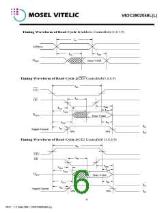
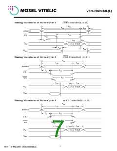
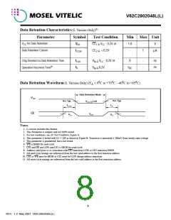
V62C2802048L(L)
0
0
0
0
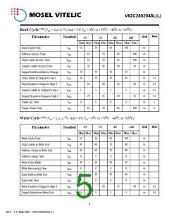
Read Cycle (3,9) (V = 2.2~2.7V, Gnd = 0V, T = 0 C to +70 C / -40 C to +85 C)
cc
A
Note
Unit
Parameter
Symbol
-55
-70
-85
-100
Min Max Min Max Min Max Min Max
t
55
-
-
70
-
-
85
-
-
100
-
100
100
50
-
ns
ns
ns
ns
ns
ns
ns
ns
ns
ns
ns
Read Cycle Time
RC
t
55
55
35
-
70
70
40
-
85
85
40
-
-
-
Address Access Time
AA
t
-
-
-
Chip Enable Access Time
Output Enable Access Time
OutputHold fromAddress Change
Chip Enable to Output in Low-Z
Chip Disable to Output in High-Z
Output Enable to Output in Low-Z
Output Disable to Output in High-Z
Power-Up Time
ACE
t
-
-
-
-
OE
t
10
10
-
10
10
-
10
10
-
10
10
-
OH
t
-
-
-
-
4,5
4,5
4,5
4,5
5
CLZ
t
25
-
30
-
35
-
40
-
CHZ
t
5
-
5
-
5
-
5
-
OLZ
t
25
-
25
-
30
-
35
-
OHZ
t
0
-
0
-
0
-
0
-
PU
t
55
70
85
100
5
Power-Down Time
PD
0
0
0
0
Write Cycle (3,11) (V = 2.2~2.7V, Gnd = 0V, T = 0 C to +70 C / -40 C to +85 C)
cc
A
Note
Unit
-55
-70
-85
-100
Parameter
Symbol
Min Max Min Max Min Max Min Max
t
55
45
45
0
-
-
70
60
60
0
-
-
85
70
70
0
-
-
100
80
80
0
-
-
ns
ns
ns
ns
ns
ns
ns
ns
ns
ns
Write Cycle Time
Chip Enable to Write End
WC
t
CW
t
-
-
-
-
Address Setup to Write End
Address Setup Time
AW
t
-
-
-
-
AS
t
45
0
-
50
0
-
60
0
-
70
0
-
Write Pulse Width
WP
t
-
-
-
-
Write Recovering Time
Data Valid to Write End
Data Hold Time
WR
t
25
0
-
30
0
-
35
0
-
40
0
-
DW
t
-
-
-
-
DH
t
-
25
-
-
30
-
-
35
-
-
40
-
4,5
4,5
Write Enable to Output in High-Z
Output Active from Write End
WZ
t
5
5
5
5
OW
5
REV. 1.2 May 2001 V62C2802048L(L)

 MOSEL [ MOSEL VITELIC, CORP ]