COMMON SPECIFICATIONS
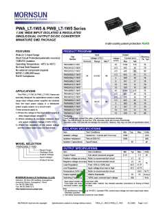
Recommended Circuit
Item
Test conditions
Min
Typ
15
Max
95
Units
%
All the PWA_LT-1W5 & PWB_LT-1W5 Series
have been tested according to the following
recommended testing circuit before leaving
factory. This series should be tested under load.
(see Figure 1).
Storage humidity range
Operating Temp. range
Storage Temp. range
Temp. rise at full load
Lead temperature
Short circuit protection
Cooling
85
-40
-55
125
°C
1.5mm from case for 10 seconds
245
Continuous, automatics recovery
Free air convection
+Vout
0V
Vin
Cin
DC DC
Case Material
MTBF
Plastic(UL94-V0)
GND
-Vout
1000
K hours
g
Single Output
Vin
Cin
+Vout
0V
Weight
5.2
DC DC
GND
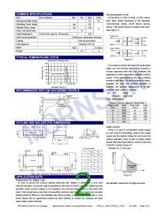
TYPICAL TEMPERATURE CUTVE
(Figure 1)
Temperature Derating Graph
If you want to further decrease the input/output
ripple, you can increase capacitance properly or
choose capacitors with low ESR. However, the
capacitance of the output filter capacitor must be
proper. If the capacitance is too big, a startup
problem might arise. For every channel of output,
provided the safe and reliable operation is
ensured, the greatest capacitance of its filter
capacitor sees (Table 1). General:
Safe Operating Area
Operating Temp.( C )
RECOMMENDED REFLOW SOLDERING PROFILE
Recommended Reflow Profile
Cin: 12V
24V&48V 10μF-47μF
Cout: 10μF/100mA
Output External Capacitor Table(Table 1)
100μF
50 Sec Max
(>220℃)
Peak.Temp 235~245℃
250
200
90 Sec Max
(>190℃)
Single Vout
(VDC)
Cout
(uF)
Dual Vout
(VDC)
Cout
(uF)
150
100
50
3.3
5
2200
1000
680
±5
±9
680
470
330
220
-
9
±12
±15
-
0
12
15
470
Time (sec.)
330
OUTLINE AND SOLDER PAD DIMENSIONS
23.86
[0.94]
15.25[0.6]
Input Current
When it is used in unregulated power supply,
be sure that the fluctuating range of the power
supply and the rippled voltage do not exceed the
module standard. Input current of power supply
should afford the flash startup current of this kind
of DC/DC module (Figure 2)
Side View
1.4
[0.055]
0.15
0.15
13.1
[0.52]
17.78[0.7]
General: Ip ≤1.4*Iin-max:
Pin Connections
0.5
[0.02]
1.02
[0.04]
Pin
1
Single
GND
Dual
GND
0.8
[0.03]
Ip
9
8
10
16
7
8
NC
NC
NC
0V
Top View
9
+Vo
0V
+Vo
-Vo
Vin
1
7
Input Voltage
Range
10
16
3.04
[0.12]
15.24
[0.60]
2.54
[0.10]
15.2
[0.60]
2.54
[0.10]
Vin
Input Voltage (V)
Note: Unit: mm[inch]; Tolerance: ±0.25mm; All Pins on a 2.54mm .
APPLICATION NOTE
Requirement On Output Load
In order to ensure the product operate efficiently and reliably, in addition to a max load
(namely full load), a minimum load is specified for this kind of DC/DC converter. Make sure the
specified range of input voltage is not exceeded, the minimum output load no less than 10%
load. If the actual load is less than the specified minimum load, the output ripple may increase
sharply while its efficiency and reliability will reduce greatly. If the actual output power is very
small, please add an appropriate resistor as extra loading, or contact our company for other
lower output power products.
No parallel connection or plug and play.
MORNSUN reserves the copyright
Specifications subject to change without notice.
PWA_LT_1W5 & PWB_LT_1W5
A/2-2008
Page 2 of 2

 MORNSUN [ MORNSUN SCIENCE& TECHNOLOGY LTD. ]