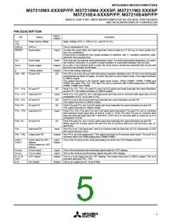
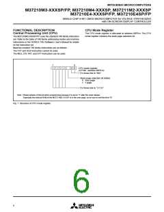
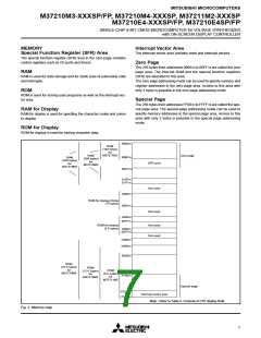
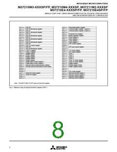
MITSUBISHI MICROCOMPUTERS
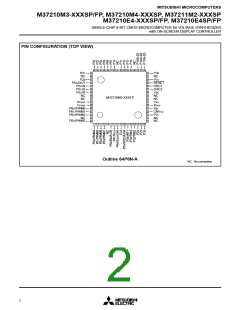
M37210M3-XXXSP/FP, M37210M4-XXXSP, M37211M2-XXXSP
M37210E4-XXXSP/FP, M37210E4SP/FP
SINGLE-CHIP 8-BIT CMOS MICROCOMPUTER for VOLTAGE SYNTHESIZER
with ON-SCREEN DISPLAY CONTROLLER
PWM OUTPUT CIRCUIT
within one period in the circuit internal section. Refer to Figure
13 (a).
(1) Introduction
Six different pulses can be output from the PWM.
The M37210M3-XXXSP/FP and M37210M4-XXXSP are
equipped with one 14-bit PWM (DA) and eight 6-bit PWMs
(PWM0-PWM7), and the M37211M2-XXXSP is equipped with
six 6-bit PWMs (PWM0-PWM5).The 14-bit resolution gives DA
the minimum resolution bit width of 500ns (for f(XIN) = 4MHz)
and a repeat period of 8192µs. PWM0-PWM7 have a 6-bit reso-
lution with minimum resolution bit width of 16ms and repeat pe-
riod of 1024µs.
These can be selected by bits 0 through 5. Depending on the
content of the 6-bit PWM latch, pulses from 5 to 0 are selected.
The PWM output is the difference of the sum of each of these
pulses. Several examples are shown in Figure 13 (b). Changes
in the contents of the PWM latch allows the selection of 64
lengths of high-level area outputs varying from 0/64 to 63/64. A
length of entirely high-level output cannot be output, i.e. 64/64.
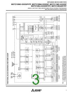
Block diagram of the PWM is shown in Figure 16.
The PWM timing generator section applies individual control
signals to DA and PWM0-7 using clock input XIN divided by 2
as a reference signal.
(5) 14-bit PWM Operation
The output example of the 14-bit PWM is shown in Figure 14.
The 14-bit PWM divides the data within the PWM latch into the
lower 6 bits and higher 8 bits.
A high-level area within a length DH times τ is output every short
area of t = 256 τ =128µs as determined by data DH of the higher
8 bits.
(2) Data Setting
The output pins PWM0-3 are in common with port P6 and
PWM4-7 are in common with port P00-P03.
Thus, the time for the high-level area is equal to the time set by
the lower 8 bits or that plus τ. As a result, the short-area period
t ( = 128µs, approx. 7.8 kHz) becomes an approximately repeti-
tive period.
For PWM output, each PWM output selection bit (bit 1 to 7 of
PWM output control register 1, bit 0, 1 of PWM output control
register 2, should be set. When DA is used for output, first set
the higher 8-bit of the DA-H register (address 00CE16), then the
lower 6-bit of the DA-L register (address 00CF16).
When one of the PWM0-7 is used for output, set the 6-bit in the
PWM0-7 register (address 00D016 to 00D416, 00F616 to
00F816), respectively.
(6) Output after Reset
At reset the output of port P6 is in the high impedance state and
the contents of the PWM register and latch are undefined. Note
that after setting the PWM register, its data is transferred to the
latch.
(3) Transferring Data from Registers to PWM
Circuit
Table 2. Relation between the low-order 6 bits of data and high-level
area increase space
The data written to the PWM registers. 8 bits of the DA-H regis-
ter is transferred to 14-bit PWM circuit when writing to lower 6
bits of the DA-L register.
6 low-order bits of data Area longer by τ than that of other tm (m = 0 to 63)
0 0 0 0 0L0SB
0 0 0 0 0 1
Nothing
m = 32
(4) Operation of the 6-bit PWMs
0 0 0 0 1 0
0 0 0 1 0 0
0 0 1 0 0 0
0 1 0 0 0 0
1 0 0 0 0 0
m = 16, 48
The timing diagram of the eight 6-bit PWMs (PWM0-7) is shown
m = 8, 24, 40, 56
m = 4, 12, 20, 28, 36, 44, 52, 60
6
in Figure 13. One period (T) is composed of 64 (2 ) segments.
There are six different pulse types configured from bits 0 to 5
representing the significance of each bit. These are output
m = 2, 6, 10, 14, 18, 22, 26, 30, 34, 38, 42, 46, 50, 54, 58, 62
m = 1, 3, 5, 7, ................................................... 57, 59, 61, 63
16

 MITSUBISHI [ Mitsubishi Group ]