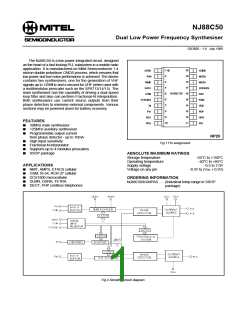
NJ88C50
The charge pump output current level is set by an external
resistor on the RSA pin (pin 9) up to a limit of 250µA +/-10%.
A pull up current pulse will indicate that the VCO frequency
must be increased, whilst a pull down pulse indicates that the
frequency must be decreased.
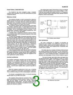
FUNCTIONAL DESCRIPTION
The NJ88C50 has been designed using a modular
concept, and its operation can be best summarised as these
component blocks.
Reference divider
The reference divider is used to provide the reference
signals needed for both the main and auxiliary synthesiser
phase detectors. The divider allows for a twelve bit number to
be loaded, via the serial bus, to select the required division
ratio. Division ratios of 3 to 4095 can be used.
The reference divider input stage will accept a low level,
AC coupled, sinewave input. It is anticipated that in most
systems this will be provided by a stable reference source up
to 35MHz, and so encompasses all the common TCXO
(temperature controlled crystal oscillator) frequencies, such
as 9.6, 12.8, 13.0, 19.44 and 26MHz.
A standby mode is supported so that the reference divider
can be powered down, this is achieved using two of the serial
program control bits.
To reduce the possibility of unwanted interaction between
the main and auxiliary synthesisers, the charge pumps do not
take current at the same time. To achieve this the output of the
reference divider has a duty factor of approximately 50:50,
which then allows the Q and QBAR taps to be used for the
auxiliary and main synthesisers respectively. By doing this the
current pulses can be taken alternatively, minimising
modulation of the power supply rails as current is drawn.
The reference divider consists of a 12 bit programmable
divider followed by a 4 bit binary counter. This 4 bit counter
gives a choice of divide by M, 2M, 4M or 8M.
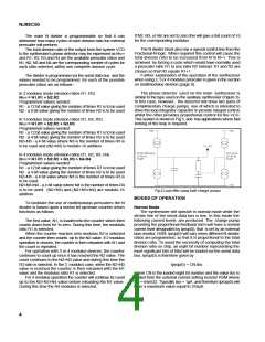
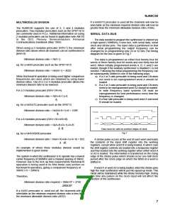
Fig.3 Auxiliary phase detector
Main Synthesiser
The main synthesiser is capable of operating at
frequencies up to 30MHz. The synthesiser uses the 12 bit
reference divider, shared with the auxiliary synthesiser, a 12
bit up/down N divider and a digital phase comparator with
current source outputs.
A pair of programmable control bits are used to determine
which of the divide by M, 2M, 4M or 8M outputs is supplied to
the auxiliary synthesiser’s phase detector and a further pair of
control bits are used to determine which are supplied to the
main synthesiser’s phase detector.
The device also has a number of features which increase
the design flexibility and performance of the synthesiser.
These include fractional-N operation, speed up mode and
support of 2, 3 and 4 modulus prescalers. A description of the
operation and advantages of each of these features is given.
Auxiliary synthesiser
The main N divider input buffer will accept inputs from
an external prescaler, either as balanced (2 wire) ECL levels
at frequencies up to 30MHz, or DC coupled to a single ended
prescaler output. Single ended operation requires the other
buffer input (pin 3) to be externally biased to the correct slicing
voltage for the prescaler and also externally decoupled.
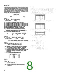
If the inputs are in the form of balanced ECL levels, there
must not be a skew of greater than 2ns between one input
changing and the second input changing. The relationship of
the signals is shown below in Fig.4.
The auxiliary synthesiser operates over an input frequency
range from 1 to 125MHz, without the use of an external
prescaler. The synthesiser consists of a 12 bit N divider and
a digital phase comparator with current source outputs. The
reference frequency is supplied by the shared reference
divider. Current source outputs allow a passive loop filter to
be used.
When the auxiliary synthesiser is not in use, a standby
mode is supported so that power consumption is reduced.
This is achieved using one of the serial program control bits.
The divider is programmed with a 12 bit word allowing
division ratios of 3 to 4095 to be used.
The auxiliary phase detector consists of the 2 D-type
phase and frequency detector shown in Figure.3 below, the
high and low outputs of which drive on-chip, opposing
complementary charge pumps. This type of phase detector
design eliminates non linearity or deadband around the zero
phase error (locked) condition.
Fig.4 Maximum input skew
3

 MITEL [ MITEL NETWORKS CORPORATION ]