MT90826 CMOS
Advanced Information
The microport interface is compatible with Motorola
Device Overview
non-multiplexed
buses.
Connection
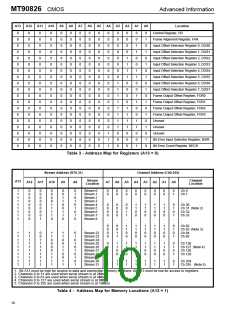
memory
locations may be directly written to or read from; data
memory locations may be directly read from. A DTA
signal is provided to hold the bus until the
asynchronous microport operation is queued into the
device. For applications that require no wait states,
indirect reading and writing may be used.
Intermediary registers are directly programmed with
the write data and address, or read address. The
data in the intermediary registers is internally
transferred synchronous with the operation of the
internal state machines. Completion of the operation
is indicated by a status register flag.
The MT90826 Quad Digital Switch is capable of
switching up to 4,096 × 4,096 channels. The
MT90826 is designed to switch 64 kbit/s PCM or N x
64k bit/s data. The device maintains frame integrity
in data applications and minimum throughput delay
for voice applications on a per channel basis.
The serial input streams of the MT90826 can have a
bit rate of 2.048, 4.096, 8.192 or 16.384 Mbit/s and
are arranged in 125µs wide frames, which contain
32, 64,128 or 256 channels, respectively. The data
rates on input and output streams match. All inputs
and outputs may be programmed to 2.048, 4.096 or
8.192 Mb/s. STi0-15 and STo0-15 may be set to
16.384 Mb/s. Combinations of two bit rates, N and
2N are provided. See Table 1.
Functional Description
A functional Block Diagram of the MT90826 is shown
in Figure 1.
By using Mitel’s message mode capability, the
microprocessor can access input and output
timeslots on a per channel basis. This feature is
useful for transferring control and status information
for external circuits or other ST-BUS devices.
Data and Connection Memory
For all data rates, the received serial data is
converted to parallel format by internal serial-to-
parallel converters and stored sequentially in the
data memory. Depending upon the selected
operation programmed in the control register, the
usable data memory may be as large as 4,096 bytes.
The sequential addressing of the data memory is
performed by an internal counter, which is reset by
the input 8 kHz frame pulse (F0i) to mark the frame
boundaries of the incoming serial data streams.
The frame offset calibration function allows users to
measure the frame offset delay for streams STi0 to
STi31. The offset calibration is activated by a frame
evaluation bit in the frame evaluation register. The
evaluation result is stored in the frame evaluation
registers and can be used to program the input offset
delay for individual streams using internal frame
input offset registers.
Data to be output on the serial streams may come
from either the data memory or connection memory.
Serial Interface Mode
Input Stream
Input Data Rate
Output Stream
Output Data Rate
8 Mb/s
16 Mb/s
STi0-31
STi0-15
STi0-15
STi15-31
STi0-11
STi12-19
STi0-31
STi0-15
STi16-31
STi0-31
8 Mb/s
16 Mb/s
4 Mbs/
8 Mb/s
16 Mb/s
8 Mb/s
4 Mb/s
2 Mb/s
4 Mb/s
2 Mb/s
STo0-31
STo0-15
STo0-15
STo16-31
STo0-11
STo12-19
STo0-31
STo0-15
STo16-31
STo0-31
8 Mb/s
16 Mb/s
4 Mb/s
8 Mb/s
16 Mb/s
8 Mb/s
4 Mb/s
2 Mb/s
4 Mb/s
2 Mb/s
4 Mb/s and 8 Mb/s
16 Mb/s and 8 Mb/s
4 Mb/s
2 Mb/s and 4 Mb/s
2 Mb/s
Table 1 - Stream Usage and External Clock Rates
6

 MITEL [ MITEL NETWORKS CORPORATION ]