MT89L86
Advance Information
Interface
Clock
required at
CLK Pin
(MHz)
Variable/
Constant
Number of
Input x
Serial
Interface
Data Rate
Matrix
Channel
Capacity
Input/Output
Streams Used
throughput
Delay
Output
Streams
Selection
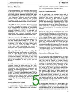
2 Mb/s
2 Mb/s
4.096
4.096
8x8
256x256 Non-Blocking
512x256 Blocking
STi0-7/STo0-7
STi0-15/STo0-7
Yes
No
16x8
2 Mb/s
4.096
4.096
10x10
8x4
128x128 Non-Blocking
(only 4-input x 4-output
can be selected)
STi0-9/STo0-9
STi0-7/STo0-3
Yes
No
Nibble
Switching
(2 Mb/s)
512x256 Nibbles
4 Mb/s
4 Mb/s
8 Mb/s
4.096
4.096
8.192
8x4
4x4
2x2
512x256 Blocking
256x256 Non-Blocking
256x256 Non-Blocking
STi0-7/STo0-3
STi0-3/STo0-3
STi0-1/STo0-1
No
Yes
Yes
Table 1 - Switching Configurations for Identical Input and Output Data Rate
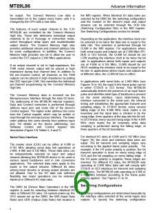
Different Input/Output Data Rates
streams for the desired operation. Table
2
summarizes the four options available when it is
used with different I/O rates. Figures 21 to 24 show
the timing for each of the four modes shown in Table
2.
When Different I/O rate is selected by the DMO bit,
the input and output data rates should be selected at
the IDR and ODR bits, respectively. The Switching
Configuration Bits (SCB) are ignored with this
operation. This selection allows the user to multiplex
conventional 2.048 Mb/s serial streams into two
higher rates and vice-versa. In addition to the rate
conversion itself, the MT89L86 allows for a complete
256 x 256 channel non-blocking switch at different
rates. In this operation, the per-channel variable/
constant throughput delay selection is provided.
Input Frame Offset Selection
For the 4.096 and 8.192 Mb/s serial interface data
rates, the MT89L86 provides a feature called Input
Frame Offset allowing the user to compensate for the
varying delays at the incoming serial inputs while
building large switch matrices. Usually, different
delays occur on the digital backbones causing the
data and frame synchronization signals to be skewed
at the input of the switch device. This may result in
the system frame synchronization pulse to be active
at the MT89L86’s FR input before the first bit of the
frame is received at the serial inputs.
Depending on which data rates are programmed for
input and output streams, the number of data
streams used on the input and output as well as the
serial interface clock (CLK input pin) is different.
Once the CPU defines the data rates at the IDR and
ODR bits, the MT89L86 automatically configures
itself with the appropriate number of input and output
Interface
Number
Variable/
Constant
Input and
Output
Data Rates
Clock
required at
CLK Pin
(MHz)
of Input
x Output
Streams
Matrix
Channel Capacity
Input/Output
Streams Used
throughput
Delay
Selection
2 Mb/s to 4 Mb/s
2 Mb/s to 8 Mb/s
4 Mb/s to 2 Mb/s
8 Mb/s to 2 Mb/s
4.096
8.192
4.096
8.192
8x4
8x2
4x8
2x8
256x256 Non-Blocking
256x256 Non-Blocking
256x256 Non-Blocking
256x256 Non-Blocking
STi0-7/STo0-3
STi0-7/STo0-1
STi0-3/STo0-7
STi0-1/STo0-7
Yes
Yes
Yes
Yes
Table 2 - Switching Configurations for Different I/O Data Rates
8

 MITEL [ MITEL NETWORKS CORPORATION ]