Preliminary Information
MT8924
Absolute Maximum Ratings*
Parameter
Symbol
Min
Max
Units
1
2
3
4
5
Supply Voltage
VDD - VSS
VI/O
- 0.3
7
VDD + 0.3
± 10
V
V
Voltage on any I/O pin
Current on any I/O pin
Storage Temperature
VSS - 0.3
II/O
mA
°C
TST
- 65
+ 150
500
Power Dissipation (plastic package)
PD
mW
* Exceeding these figures may cause permanent damage. Functional operation under these conditions is not guaranteed.
Recommended Operating Conditions
Characteristics
Supply Voltage
Sym
Min
Typ*
Max
Units
Test Conditions
1
2
3
VDD
TOP
VIH
4.75
0
5
5.25
+70
VDD
V
°C
V
Ambient Operating Temp. Range
Input Voltage High
2.4
for 400mv noise
margin
4
Input Voltage Low
VIL
VSS
0.8
V
* Typical figures are at 25°C and are for design aid only; not guaranteed and not subject to production testing.
DC Characteristics: Clocked operation (TOP=0 to 70°C; VDD=5V 5%)
Characteristics
Input Low Level
Sym
VIL
Min
Typ
Max
Units
Test Conditions
1
2
3
4
5
6
0.8
V
V
Pins 1-3, 6-13, 15-20, 22-23
Pins 1-3, 6-13, 15-20, 22-23
Pins 4, 6-13; IOL=4 mA
Pins 4, 6-13; IOL=4 mA
Pins 5, 21; IOL=8 mA
VIH
VOL
VOH
VOL
IIL
Input High Level
2.0
2.4
Output Low Level
Output High Level
Output Low Level
Input Leakage Current
0.4
V
V
0.4
10
V
µA
Pins 1-3, 6-13, 15-20, 22-23;
VIN=0 to VDD
7
Data Bus Leakage Current
IOL
10
10
µA
Pins 6-13; VIN=0 to VDD
CS=VDD
;
8
Supply Current
IDD
mA
Pin 14; Cki=4.096 MHz
All DC characterisitics are valid 250µs after V
and C4i have been applied.
DD
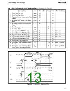
AC Electrical Characteristics - Capacitances
Characteristics
Input Capacitance
Sym
Min
Typ
Max
Units
Test Conditions
1
2
3
CI
CI/O
CO
5
pF
pF
pF
frequency=1MHz; TOP=0
to 70°C;
unused pins tied to VSS;
VDD=5V±5%
I/O Capacitance (Bidirectional)
Output Capacitance
15
10
8-11

 MITEL [ MITEL NETWORKS CORPORATION ]