Preliminary Information
MH89760B
The received data is written into the elastic buffer
with the extracted 1.544 MHz clock. The data is read
out of the buffer on the ST-BUS side with the system
2.048 MHz clock. The maximum delay through the
buffer is 1.3 ST-BUS frames (i.e., 42 ST-BUS
channels). The minimum delay required to avoid bus
contention in the buffer memory is two ST-BUS
channels.
ESF or SLC-96 mode will, however, undergo slips at
the same time.
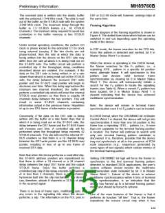
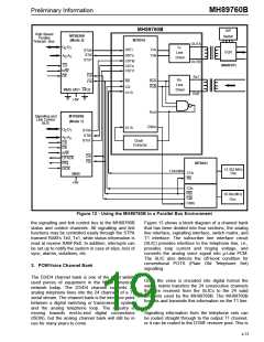
Framing Algorithm
A state diagram of the framing algorithm is shown in
Figure 8. The dotted lines show which feature can be
switched in and out depending upon the operating
mode of the device.
Under normal operating conditions, the system C2i
clock is phase locked to the extracted E1.5o clock
using external circuitry. If the two clocks are not
phase-locked, then the rate at which the data is
being written into the device on the DS1 side may
differ from the rate at which it is being read out on
the ST-BUS side. The buffer circuit will perform a
controlled slip if the throughput delay conditions
described above are violated. For example, if the
data on the DS1 side is being written in at a rate
slower than what it is being read out on the ST-BUS
side, the delay between the received DS1 write
pointer and the ST-BUS read pointer will begin to
decrease over time. When this delay approaches the
minimum two channel threshold, the buffer will
perform a controlled slip which will reset the internal
ST-BUS read pointers so that there is exactly 34
channels delay between the two pointers. This will
result in some ST-BUS channels containing
information output in the previous frame. Repetition
of up to one DS1 frame of information is possible.
In ESF mode, the framer searches for the FPS bits.
Once this pattern is detected and verified, bit 0 in
Master Status Word 1 is cleared.
When the device is operating in the D3/D4 format,
the framer searches for the FT pattern, i.e., a
repeating 1010... pattern in a specific bit position
every alternate frame. It will synchronize to this
pattern
and
declare
valid
terminal
frame
synchronization by clearing bit 0 in Master Status
Word 1. The device will subsequently initiate a
search for the FS pattern to locate the signalling
frames (see Table 4). When a correct FS pattern has
been located, bit 3 in Master Status Word 1 is
cleared indicating that the device has achieved
multiframe synchronization.
Note: the device will remain in terminal frame
synchronization even if no FS pattern can be located.
Conversely, if the data on the DS1 side is being
written into the buffer at a rate faster than that at
which it is being read out on the ST-BUS side, the
delay between the DS1 frame and the ST-BUS frame
will increase over time. A controlled slip will be
performed when the throughput delay exceeds 42
ST-BUS channels. This slip will reset the internal ST-
BUS counters so that there is a 10 channel delay
between the DS1 write pointer and the ST-BUS read
pointer, resulting in loss of up to one frame of
received DS1 data.
In D3/D4 format, when the CRC/MIMIC bit in Master
Control Word 1 is cleared, the device will not go into
synchronization if more than one bit position in the
frame has a repeating 1010.... pattern, i.e., if more
than one candidate for the terminal framing position
is located. The framer will continue to search until
only one terminal framing pattern candidate is
discovered. It is, therefore, possible that the device
may not synchronize at all in the presence of PCM
code sequences (e.g., sequences generated by
some types of test signals) which contain mimics of
the terminal framing pattern.
Note that when the device performs a controlled slip,
the ST-BUS address pointers are repositioned so
that there is either a 10 channel or a 34 channel
delay between the input DS1 frame and the output
Setting CRC/MIMIC bit high will force the framer to
synchronize to the first terminal framing pattern
detected. In standard D3/D4 applications, the user’s
system software should monitor the multiframe
synchronization state indicated by bit 3 in Master
Status Word 1. Failure of the device to achieve
multiframe synchronization within 4.5ms of terminal
frame synchronization, is an indication that the
device has framed up to a terminal framing pattern
mimic and should be forced to reframe.
ST-BUS frame. Since the buffer performs
a
controlled slip only if the delay exceeds 42 channels
or is less than 2 channels, there is an 8 channel
hysteresis built into the slip mechanism. The device
can, therefore, absorb 8 channels or 32.5µs of jitter
in the received signal.
There is no loss of frame sync, multiframe sync or
any errors in the signalling bits when the device
performs a slip. The information on the FDL pins in
One of the main features of the framer is that it
performs its function "off line". That is, the framer
repositions the receive circuit only when it has
4-69

 MITEL [ MITEL NETWORKS CORPORATION ]