8.0-12.0/16.0-24.0 GHz GaAs MMIC
Active Doubler
January 2007 - Rev 17-Jan-07
X1005-BD
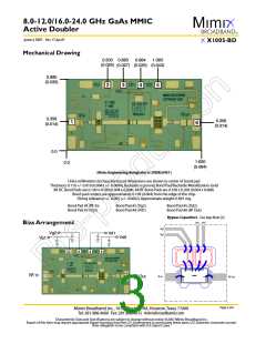
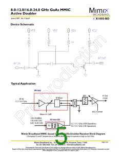
Mechanical Drawing
0.503
0.683
0.884
1.085
(0.020)
(0.027) (0.035) (0.043)
0.890
(0.035)
2
3
4
5
XX1005-BD
0.356
0.356
1
6
(0.014)
(0.014)
0.0
1.620
0.0
(0.064)
(Note: Engineering designator is 20DBL0451)
Units: millimeters (inches) Bond pad dimensions are shown to center of bond pad.
Thickness: 0.110 +/- 0.010 (0.0043 +/- 0.0004), Backside is ground, Bond Pad/Backside Metallization: Gold
All DC Bond Pads are 0.100 x 0.100 (0.004 x 0.004). All RF Bond Pads are 0.100 x 0.200 (0.004 x 0.008)
Bond pad centers are approximately 0.109 (0.004) from the edge of the chip.
Dicing tolerance: +/- 0.005 (+/- 0.0002). Approximate weight: 0.891 mg.
Bond Pad #1 (RF In)
Bond Pad #2 (Vg1)
Bond Pad #3 (Vg2)
Bond Pad #4 (Vd1)
Bond Pad #5 (Vd2)
Bond Pad #6 (RF Out)
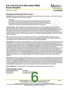
Bypass Capacitors - See App Note [2]
Vd1 Vd2
Bias Arrangement
Vg2
Vg1
Vg2
Vd1
Vd2
Vg1
2
3
4
5
XX1005-BD
RF In
1
6
RF In
RF Out
RF Out
Page 3 of 6
Mimix Broadband, Inc., 10795 Rockley Rd., Houston,Texas 77099
Tel: 281.988.4600 Fax: 281.988.4615 mimixbroadband.com
Characteristic Data and Specifications are subject to change without notice. ©2007 Mimix Broadband, Inc.
Export of this item may require appropriate export licensing from the U.S. Government. In purchasing these parts, U.S. Domestic customers accept
their obligation to be compliant with U.S. Export Laws.

 MIMIX [ MIMIX BROADBAND ]