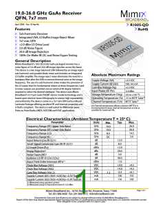
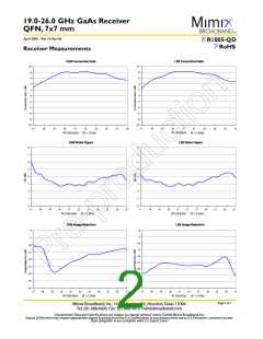
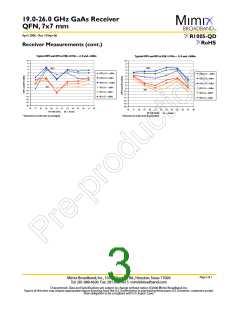
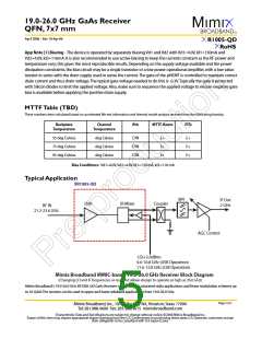
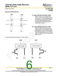
19.0-26.0 GHz GaAs Receiver
QFN, 7x7 mm
April 2006 - Rev 10-Apr-06
R1005-QD
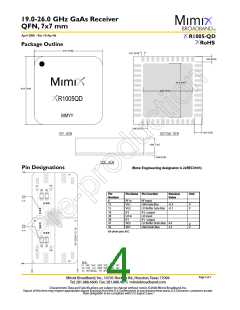
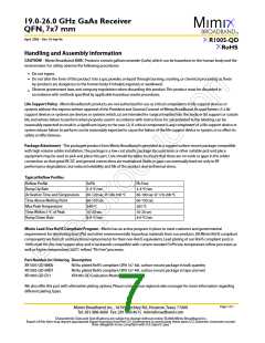
Package Outline
Pin Designations
(Note: Engineering designator is 22REC0393)
Pin
Number
Pin Name Pin Function
Nominal
Value
Unit
6
13
15
RF in
VG1
VG2
RF input
LNA Gate Bias
LO Buffer Gate Bias -0.1
-0.3
V
V
18
28
38
41
43
IF2 output
LO input
IF1 output
LO Buffer Drain Bias 4.0
IF2
LO in
IF1
VD2
VD1
V
V
LNA Drain Bias
3.5
All other pins N/C
Page 4 of 7
Mimix Broadband, Inc., 10795 Rockley Rd., Houston,Texas 77099
Tel: 281.988.4600 Fax: 281.988.4615 mimixbroadband.com
Characteristic Data and Specifications are subject to change without notice. ©2006 Mimix Broadband, Inc.
Export of this item may require appropriate export licensing from the U.S. Government. In purchasing these parts, U.S. Domestic customers accept
their obligation to be compliant with U.S. Export Laws.

 MIMIX [ MIMIX BROADBAND ]