12.0-16.0 GHz Power Amplifier
QFN, 3x3mm
February 2008 - Rev 10-Feb-08
P1042-QT
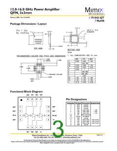
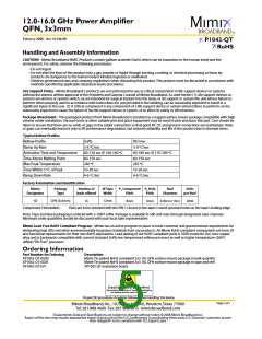
Package Dimensions / Layout
Functional Block Diagram
gnd Vd1 Vd2 Vd3
Pin Designations
Pin Number Pin Name Pin Function Nominal Value
1-2
3
4
5
6
GND
RF In
GND
Vg1
Vg2
Vg3
Ground
RF Input
Ground
gnd
gnd
1
2
3
4
12
11
10
9
gnd
gnd
Gate 1 Bias
Gate 2 Bias
Gate 3 Bias
Not Connected
RF Output
Ground
Drain 3 Bias
Drain 2 Bias
Drain 1 Bias
Ground
~ -1.0V
~ -0.8V
~ -1.0V
7
8-9
10
11-12
13
14
15
16
NC
RF In
gnd
RF Out
nc
RF Out
GND
Vd3
Vd2
Vd1
5.0V, 250 mA
5.0V, 125 mA
5.0V, 125 mA
GND
Vg1 Vg2 Vg3
nc
Page 3 of 5
Mimix Broadband, Inc., 10795 Rockley Rd., Houston,Texas 77099
Tel: 281.988.4600 Fax: 281.988.4615 mimixbroadband.com
Characteristic Data and Specifications are subject to change without notice. ©2008 Mimix Broadband, Inc.
Export of this item may require appropriate export licensing from the U.S. Government. In purchasing these parts, U.S. Domestic customers accept
their obligation to be compliant with U.S. Export Laws.

 MIMIX [ MIMIX BROADBAND ]