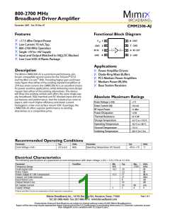
800-2700 MHz
Broadband Driver Amplifier
December 2007 - Rev 29-Dec-07
CMM2306-AJ
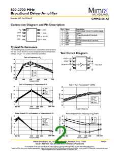
Connection Diagram and Pin Description
Pin # Name
Description
Drain voltage. Connect to positive suppl.y
V
1
2
3
4
8
7
6
5
GND
d
1
+V
d
GND
RF IN
GND
GND
2
3
4
5
6
7
8
GND
RF IN
GND
GND
RF OUT
GND
GND
Ground.
RF input (Internally DC blocked).
Ground.
Ground.
RF output (Internally DC blocked).
Ground.
Ground.
RF OUT
GND
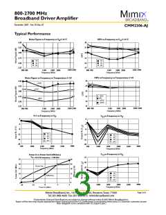
Typical Performance
The following typical performance parameters were tested in
the test circuit shown at room temperature and with a drain
Test Circuit Diagram
voltage (+V ) = 5 V, unless otherwise specified.
d
1
8
7
6
5
Gain vs Frequency vs V
d
+5V
30
2
0.01µF
3
26
22
RF IN
RF OUT
4
18
14
10
3V
4V
5V
6V
3000
500
1000
1500
2000
2500
Frequency (MHz)
Gain vs Frequency vs Temperature @ 5V
Gain vs V vs Temperature@ 1.8 GHz
d
32
29
26
23
30
28
26
24
-20°C
0°C
+25°C
+70°C
-20°C
0°C
+25°C
+70°C
20
17
22
20
2400 2500
800 900
1500
Frequency (MHz)
1800 2000
6
3
4
5
Supply Voltage (V
)
d
Power Output (P-1) vs Frequency vs Temperature @ 5V
Power Output (P-1) vs Frequency vs V @ 25 °C
d
21
20
19
18
24
21
18
15
3V
5V
6V
-20°C
0°C
+25°C
+70°C
17
16
12
9
2400 2500
2400 2500
800 900
1500
1800 2000
800 900
1500
1800 2000
Frequency (MHz)
Frequency (MHz)
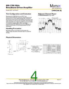
Page 2 of 5
Mimix Broadband, Inc., 10795 Rockley Rd., Houston,Texas 77099
Tel: 281.988.4600 Fax: 281.988.4615 mimixbroadband.com
Characteristic Data and Specifications are subject to change without notice. ©2007 Mimix Broadband, Inc.
Export of this item may require appropriate export licensing from the U.S. Government. In purchasing these parts, U.S. Domestic customers accept
their obligation to be compliant with U.S. Export Laws.

 MIMIX [ MIMIX BROADBAND ]