66012
FOUR CHANNEL, HERMETICALLY SEALED, LOW-INPUT CURRENT, 6N140 OPTOCOUPLER
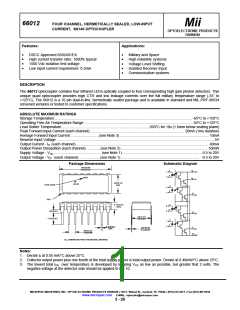
ELECTRICAL CHARACTERISTICS
°
°
Ta = -55 C to 125 C unless otherwise specified.
PARAMETER
SYMBOL
MIN
300
300
200
TYP
1000
750
400
0.1
MAX
UNITS
TEST CONDITIONS
NOTE
1,2
1,2
1,2
1
Current Transfer Ratio
CTR
%
%
%
V
I = 0.5mA, V = 0.4V, V = 4.5V
F O CC
F
F
I = 1.6mA, V = 0.4V, V = 4.5V
O
CC
I = 5.0mA, V = 0.4V, V = 4.5V
O
CC
Logic Low Output Voltage
V
OL
0.4
0.4
250
40
4
1.8
I = 0.5mA, I = 1.5mA, V = 4.5V
F
OL
CC
0.2
V
I = 5.0mA, I = 10mA, V = 4.5V
F CC
OL
I = 2µA, V = V = 18V
Logic High Output Current
High Level Output Current
Low Level Supply Current
Input Forward Voltage
I
.005
.010
2
µA
µA
mA
V
V
µA
1,3
OH
F
O
CC
I
I
=I =I =I = 0mA, V = 18V
CCH
F1 F2 F3 F4 CC
I
I = I = I = I =1.6mA, V = 18V
CCL
F1 F2 F3 F4 CC
V
1.4
I
= 1.6mA
I = 10µA
R
1
1
4
F
F
Input Reverse Breakdown Voltage
Input-Output Insulation Leakage
Current
BV
5
R
I
1.0
V
I—0
= 1500Vdc,
I—O
Relative Humidity = 45%
= 25°C, t = 5s
t
A
Propagation Delay Time To High
Output Level
Propagation Delay Time To Low
Output Level
t
t
5
4
8
2
60
30
100
10
µs
µs
µs
µs
I = 0.5mA, V = 5.0V, R = 4.7kΩ
PLH
F
CC
L
I = 5mA, V = 5.0V, R = 680kΩ
F
CC
L
I
I
= 0.5mA, V = 5.0V, R = 4.7kΩ
PHL
F
F
CC
L
= 5mA, V = 5.0V, R = 680kΩ
CC
L
°
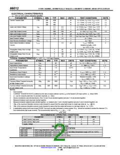
TYPICAL CHARACTERISTICS Ta = 25 C, VCC = 5V Each Channel
PARAMETER
SYMBOL
MIN
TYP
MAX
UNITS
pF
pF
TEST CONDITIONS
NOTE
°
Input Capacitance
C
C
∆vF
∆TA
R
R
60
V
F
= 0, f = MHz, t = 25 C
a
1
1, 5
1
IN
°
Capacitance (Input-Output)
Input Diode Temperature
Coefficient
Resistance (Input-Output)
Resistance (Input-Input)
Input-Input Insulation Leakage
Current
1.5
-1.8
f = 1MHz, t = 25 C
I-O
a
°
mV/ C
I = 1.6mA
F
12
°
10
10
0.5
Ω
Ω
VI
V
= 500V, t = 25 C
a
1, 5
6
6
I-0
—O
12
°
= 500V, t = 25 C
I-I
I—I
a
I
nA
Relative Humidity = 45%
= 500V, t = 5s
I-I
V
I—I
Common Mode Transient immunity
at High Output Level
Common Mode Transient Immunity
at Low Output Level
NOTES:
CM
500
500
1000
1000
V/µs
V/µs
V
V
= 50V P-P ,V
= 5.0V,
7,9
8,9
H
CM
R
CC
= 1.5kΩ, I = OmA
L
F
CM
= 50V P-P ,V
= 5.0V,
L
CM
CC
= 1.5kΩ, I = 1.6mA
R
L
F
1.
2.
3.
4.
5.
6.
7.
8.
9.
Each channel.
CURRENT TRANSFER RATIO is defined as the ratio of output collector current, I , to the forward LED input current., I , times 100%.
F
Device considered a two-terminal device. Pins 1-6 and 16 are shorted together and pins 7-14 are shorted together.
Measured between each input pair shorted together.
O
F
I = 2µA for channel under test. For all other channels, I = 10mA.
F
Measured between adjacent pairs shorted together, i.e. between pins 1 and 2 shorted together and pins 3 and 4 shorted together, etc.
CM is the maximum tolerable common mode transient to assure that the output will remain in a high logic state (ie. V > @.0V).
H
O
O
CM is the maximum tolerable common mode transient to assure that the output will remain in a low logic state (ie. V < 0.8V).
L
In applications where dv/dt may exceed 50,000 V/µs (such as static discharge) a series resistor, R , should be included to protect the detector IC”s
CC
from destructively high surge currents. The recommended value is R
=
1V
= kΩ
CC
0.6I (mA)
F
RECOMMENDED OPERATING CONDITIONS:
PARAMETER
Input Current, Low Level
SYMBOL
MIN
0
MAX
2
UNITS
µA
I
FL
Input Current, High Level
Supply Voltage
I
0.5
2.0
5
18
mA
V
FH
V
SELECTICOCN GUIDE
PART NUMBER
PART DESCRIPTION
66012-001
66012-002
66012-003
66012-004
DSCC Dwg 8302401EX Quad Channel Optocoupler
Quad Channel optocoupler, commercial, tested over full military temperature range (-55 C to +125 C)
Quad Channel optocoupler, commercial (0 to +70 C)
°
°
°
°
°
°
Quad Channel optocoupler, commercial (-40 C to +85 C)
MICROPAC INDUSTRIES, INC. OPTOELECTRONIC PRODUCTS DIVISION • 725 E. Walnut St., Garland, TX 75040 • (972) 272-3571 • Fax (972) 487-6918
www.micropac.com E-MAIL: optosales@micropac.com
3 - 28

 MII [ Micropac Industries ]