S-Type Voltage Controlled Crystal Oscillator
Performance Characteristics
Table 1. Electrical Performance
Parameter
Symbo
Min
Typical
Maximum
Units
l
Supply Voltage 1 (+5 or +3.3 V)
Supply Current
VDD
IDD
0.9*VDD
1.1*VDD
V
10mA +0.25mA/MHz
mA
Output Logic Levels
Output Logic High2
VOH
VOL
0.8*VDD
V
V
Output Logic Low2
0.1VDD
Transition Times
Rise Time2
tR
tF
SYM
fO
VC
VC
5
5
ns
ns
%
MHz
V
V
Fall Time2
Symmetry or Duty Cycle3
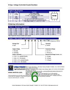
Nominal Output Frequency Options
Test Conditions for APR (+5V option)
Test Conditions for APR (+3.3V option)
Absolute Pull Range (ordering option)
Gain Transfer
45/55
65.536
4.5
1.024
0.5
0.3
3.0
APR
50,80 or 100
Positive
ppm
Operating temperature (ordering option)
Control Voltage Leakage Current
Control Voltage Bandwidth (-3dB)
0/70 or –40/85
°C
uA
KHz
IVCXO
BW
±1
10
1. A 0.01uF capacitor should be located as close to the supply as possible (to ground) and a 0.1uF is also recommended.
2. Figure 1 defines these parameters. Figure 2 illustrates the equivalent five gate TTL load and operating conditions under which
these parameters are tested and specified.
3. Symmetry is defined as (ON TIME/PERIOD with Vs=-1.4 V for TTL and Vs=2.5 V for CMOS, 5 volt operation, and Vs=1.65V for
3.3 Volt operation. TTL/CMOS pin should be grounded for frequencies <12MHz.
TF
TR
IDD
650Ω
80%
50%
20%
6
1
2
5
3
+
-
4
VDD
.01µF
.1µF
IC
VC
On Time
15pF
1.8k
+
-
Period
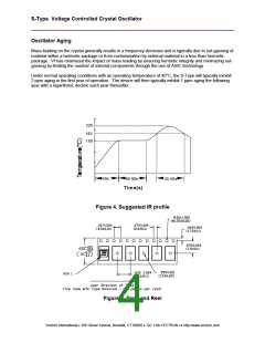
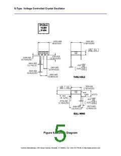
Figure 2. Output Waveform
Figure 3. Output Test Conditions (25±5°C)
Absolute Maximum Ratings
Stresses in excess of the absolute maximum ratings can permanently damage the device. Functional
operation is not implied at these or any other conditions in excess of conditions represented in the
operational sections of this data sheet. Exposure to absolute maximum ratings for extended periods may
adversely affect device reliability.
Table 2. Absolute Maximum Ratings
Parameter
Power Supply
Storage Temperature
Voltage Control Range
Symbol
VDD
Tstorage
VC
Ratings
7
-55/125
0 to VDD
Unit
Vdc
°C
V
Vectron International 166 Glover Avenue, Norwalk CT 06856-5160 Tel:1-88-VECTRON-1
vectron@vectron.com
e-mail:

 MICROSEMI [ Microsemi ]