P RODUCT DATABOOK 1 9 9 6 / 1 9 9 7
MC33164-3/ MC34164-3
3 V UNDERVOLTAGE
S
ENS I NG
CI RCUI T
P R O D U C T I O N D A T A S H E E T
A B S O LU TE M A X I M U M R ATI N G S
(Note 1 )
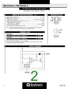
PACKAG E P IN O UTS
Input Supply Voltage (V ) ............................................................................... -1V to 12V
IN
N.C.
N.C.
N.C.
N.C.
RESET
1
2
3
4
8
7
6
5
RESET Output Voltage (VOUT) ..................................................................................... 12V
Output Sink Current (IOL) ............................................................ Internally Limited (mA)
Clamp Diode Forward Current (IF), Pin 1 to pin 2 ............................................... 100mA
Operating Junction Temperature
Plastic (DM, LP - Packages) .................................................................................. 150°C
Storage Temperature Range ...................................................................... -65°C to 150°C
Lead Temperature (Soldering, 10 seconds) ............................................................. 300°C
V
IN
N.C.
GROUND
DM PACKAGE
(Top View)
Note 1. Values beyond which damage may occur. All voltages are specified with respect to
ground, and all currents are positive into the specified terminal.
3. GROUND
2.
1. RESET
V
IN
TH ER M A L D ATA
DM PACKAGE:
THERMAL RESISTANCE-JUNCTION TO AMBIENT, θJA
LP PACKAGE:
165°C/W
156°C/W
LP PACKAGE
(Top View)
THERMAL RESISTANCE-JUNCTION TO AMBIENT, θJA
Junction Temperature Calculation: TJ = TA + (PD x θJA).
The θJA numbers are guidelines for the thermal performance of the device/pc-board system.
All of the above assume no ambient airflow
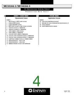
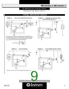
B LO CK D I A G R A M
V
IN
RESET
1.2 VREF
GROUND
Copyright © 1999
Rev. 1.2 6/ 99
2

 MICROSEMI [ Microsemi ]