HAL82x
DATA SHEET
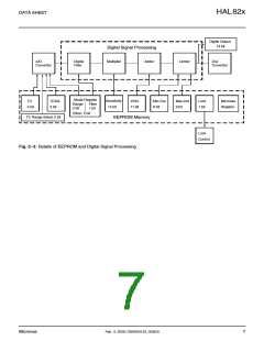
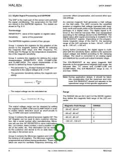
2.2. Digital Signal Processing and EEPROM
converter offset compensation, and several other spe-
cial settings.
The DSP is the main part of this sensor and performs
the signal conditioning. The parameters for the DSP
are stored in the EEPROM registers. The details are
shown in Fig. 2–3.
An external magnetic field generates a Hall voltage
on the Hall plate. The ADC converts the amplified
positive or negative Hall voltage (operates with mag-
netic north and south poles at the branded side of the
package) to a digital value. The digital signal is fil-
tered in the internal low-pass filter and manipulated
according to the settings stored in the EEPROM. The
digital value after signal processing is readable in the
D/A-READOUT register. Depending on the program-
mable magnetic range of the Hall IC, the operating
range of the A/D converter is from −30 mT...+30 mT
up to −100 mT...+100 mT.
Terminology:
SENSITIVITY: name of the register or register value
Sensitivity:
name of the parameter
The EEPROM registers consist of four groups:
Group 1 contains the registers for the adaption of the
sensor to the magnetic system: MODE for selecting
the magnetic field range and filter frequency, TC,
TCSQ and TC-Range for the temperature characteris-
tics of the magnetic sensitivity.
During further processing, the digital signal is multi-
plied with the sensitivity factor, added to the quiescent
output voltage and limited according to the clamping
voltage. The result is converted to an analog signal
and stabilized by a push-pull output transistor stage.
Group 2 contains the registers for defining the output
characteristics: SENSITIVITY, VOQ, CLAMP-LOW,
and CLAMP-HIGH. The output characteristic of the
sensor is defined by these 4 parameters.
The D/A-READOUT at any given magnetic field
depends on the programmed magnetic field range, the
low-pass filter, TC values and CLAMP-LOW and
CLAMP-HIGH. The D/A-READOUT range is min. 0
and max. 16383.
– The parameter VOQ (Output Quiescent Voltage) cor-
responds to the output voltage at B = 0 mT.
– The parameter Sensitivity defines the magnetic sen-
sitivity:
Note: During application design, it should be taken
into consideration that the maximum and mini-
mum D/A-READOUT should not saturate in the
operational range of the specific application.
ΔVOUT
-----------------
Sensitivity =
ΔB
– The output voltage can be calculated as:
Range
The RANGE bits are bit 2 and 3 of the MODE register;
they define the magnetic field range of the A/D con-
verter.
VOUT Sensitivity × B + VOQ
Magnetic Field Range
−30 mT...30 mT
RANGE
The output voltage range can be clamped by setting
the registers CLAMP-LOW and CLAMP-HIGH in order
to enable failure detection (such as short-circuits to
VDD or GND and open connections).
0
1
2
3
−60 mT...60 mT
Group 3 contains the general purpose register GP. The
GP Register can be used to store customer informa-
tion, like a serial number after manufacturing. Micro-
nas will use this GP REGISTER to store informations
like, Lot number, wafer number, x and y position of the
die on the wafer, etc. This information can be readout
by the customer and stored in it’s on data base or it
can stay in the sensor as is.
−80 mT...80 mT
−100 mT...100 mT
Group 4 contains the Micronas registers and LOCK for
the locking of all registers. The Micronas registers are
programmed and locked during production. These reg-
isters are used for oscillator frequency trimming, A/D
8
Feb. 3, 2009; DSH000143_003EN
Micronas

 MICRONAS [ MICRONAS ]