256Mb, 512Mb, 1Gb, 2Gb: 3V Embedded Parallel NOR Flash
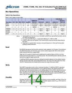
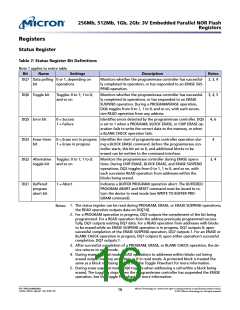
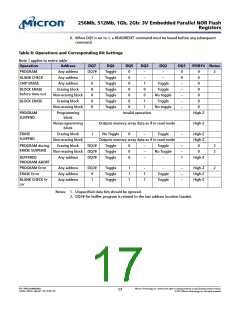
Registers
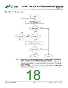
Figure 5: Data Polling Flowchart
Start
Read DQ7, DQ5, and DQ1
at valid address1
Yes
DQ7 = Data
No
No
No
DQ5 = 1
Yes
DQ1 = 1
Yes
Read DQ7 at valid address
Yes
DQ7 = Data
No
Failure2
Success
1. Valid address is the address being programmed or an address within the block being
erased or on which a BLANK CHECK operation has been executed.
Notes:
2. The data polling process does not support the BLANK CHECK operation. The process
represented in the Toggle Bit Flowchart figure can provide information on the BLANK
CHECK operation.
3. Failure results: DQ5 = 1 indicates an operation error; DQ1 = 1 indicates a WRITE TO BUF-
FER PROGRAM ABORT operation.
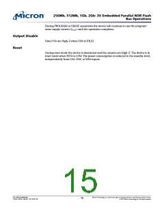
PDF: 09005aef849b4b09
m29ew_256mb_2gb.pdf - Rev. B 8/12 EN
Micron Technology, Inc. reserves the right to change products or specifications without notice.
18
© 2012 Micron Technology, Inc. All rights reserved.

 MICRON [ MICRON TECHNOLOGY ]