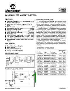
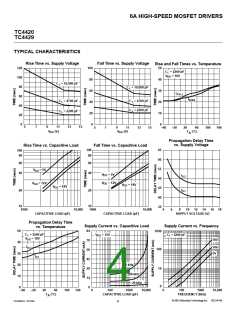
6A HIGH-SPEED MOSFET DRIVERS
TC4420
TC4429
Storage Temperature Range ................ – 65°C to +150°C
Operating Temperature (Chip) .............................. +150°C
Operating Temperature Range (Ambient)
C Version ............................................... 0°C to +70°C
I Version ........................................... – 25°C to +85°C
E Version .......................................... – 40°C to +85°C
M Version ....................................... – 55°C to +125°C
Lead Temperature (Soldering, 10 sec) ................. +300°C
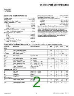
ABSOLUTE MAXIMUM RATINGS*
Supply Voltage ......................................................... +20V
Input Voltage ............................................... – 5V to > VDD
Input Current (VIN > VDD) .........................................50mA
Power Dissipation, (TA ≤ 70°C)
PDIP ...............................................................730mW
SOIC ...............................................................470mW
CerDIP ............................................................800mW
5-Pin TO-220 ......................................................1.6W
Package Power Dissipation, TC ≤ 25°C
*Static-sensitive device. Unused devices must be stored in conductive
material. Protect devices from static discharge and static fields.
Stresses above those listed under "Absolute Maximum Ratings" may
cause permanent damage to the device. These are stress ratings only
and functional operation of the device at these or any other conditions
above those indicated in the operation sections of the specifications is
not implied. Exposure to absolute maximum rating conditions for
extended periods may affect device reliability.
5-Pin TO-220 (With Heat Sink) .........................12.5W
Derating Factors (To Ambient)
PDIP ............................................................. 8mW/°C
SOIC ............................................................. 4mW/°C
CerDIP ....................................................... 6.4mW/°C
5-Pin TO-220 .............................................. 12mW/°C
Thermal Impedances (To Case)
5-Pin TO-220 RθJ-C ...................................................... 10°C/W
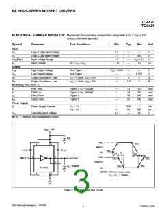
ELECTRICAL CHARACTERISTICS: TA = +25°C with 4.5V ≤ VDD ≤ 18V, unless otherwise specified.
Symbol
Parameter
Test Conditions
Min
Typ
Max
Unit
Input
VIH
Logic 1 High Input Voltage
Logic 0 Low Input Voltage
Input Voltage Range
Input Current
2.4
—
1.8
1.3
—
—
0.8
V
VIL
V
VIN (Max)
IIN
– 5
– 10
VDD +0.3
10
V
0V ≤ VIN ≤ VDD
—
µA
Output
VOH
VOL
High Output Voltage
Low Output Voltage
See Figure 1
VDD – 0.025
—
—
2.1
1.5
6
—
0.025
2.8
2.5
—
V
V
Ω
Ω
A
A
See Figure 1
—
—
RO
Output Resistance, High
Output Resistance, Low
Peak Output Current
IOUT = 10 mA, VDD = 18V
IOUT = 10 mA, VDD = 18V
VDD = 18V (See Figure 5)
RO
—
IPK
—
IREV
Latch-Up Protection
Withstand Reverse Current
Duty Cycle ≤ 2%
t ≤ 300µsec
1.5
—
—
Switching Time (Note 1)
tR
Rise Time
Figure 1, CL = 2500pF
Figure 1, CL = 2500pF
Figure 1
—
—
—
—
25
25
55
55
35
35
75
75
nsec
nsec
nsec
nsec
tF
Fall Time
tD1
Delay Time
Delay Time
tD2
Figure 1
Power Supply
IS
Power Supply Current
Operating Input Voltage
VIN = 3V
VIN = 0V
—
—
0.45
55
1.5
150
mA
µA
VDD
4.5
—
18
V
© 2001 Microchip Technology Inc. DS21419A
TC4420/9-6 10/18/96
2

 MICROCHIP [ MICROCHIP ]