PIC18F2480/2580/4480/4580
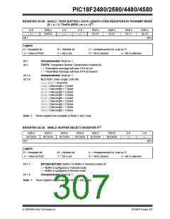
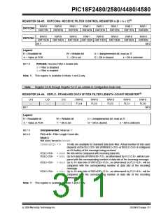
REGISTER 24-45: RXFCONn: RECEIVE FILTER CONTROL REGISTER n [0 ≤ n ≤ 1](1)
R/W-0
R/W-0
R/W-1
R/W-1
R/W-1
R/W-1
R/W-1
R/W-1
RXFCON0
RXF7EN
RXF6EN
RXF5EN
RXF4EN RXF3EN
RXF2EN
RXF1EN
RXF0EN
R/W-0
R/W-0
R/W-0
R/W-1
R/W-0
R/W-0
R/W-0
R/W-0
RXFCON1
RXF15EN
RXF14EN
RXF13EN RXF12EN RXF11EN RXF10EN
RXF9EN
RXF8EN
bit 7
bit 0
Legend:
R = Readable bit
-n = Value at POR
W = Writable bit
‘1’ = Bit is set
U = Unimplemented bit, read as ‘0’
‘0’ = Bit is cleared x = Bit is unknown
bit 7-0
RXFnEN: Receive Filter n Enable bits
0= Filter is disabled
1= Filter is enabled
Note 1: This register is available in Mode 1 and 2 only.
Note:
Register 24-46 through Register 24-51 are writable in Configuration mode only.
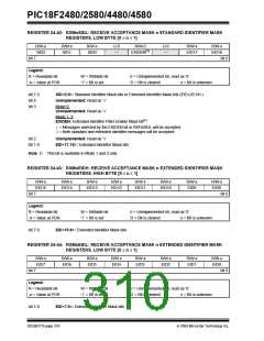
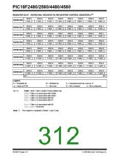
REGISTER 24-46: SDFLC: STANDARD DATA BYTES FILTER LENGTH COUNT REGISTER(1)
U-0
—
U-0
—
U-0
—
R/W-0
FLC4
R/W-0
FLC3
R/W-0
FLC2
R/W-0
FLC1
R/W-0
FLC0
bit 0
bit 7
Legend:
R = Readable bit
-n = Value at POR
W = Writable bit
‘1’ = Bit is set
U = Unimplemented bit, read as ‘0’
‘0’ = Bit is cleared x = Bit is unknown
bit 7-5
bit 4-0
Unimplemented: Read as ‘0’
FLC<4:0>: Filter Length Count bits
Mode 0:
Not used; forced to ‘00000’.
00000-10010 = 0
18 bits are available for standard data byte filter. Actual number of bits used
depends on the DLC<3:0> bits (RXBnDLC<3:0> or BnDLC<3:0> if configured
as RX buffer) of the message being received.
If DLC<3:0> = 0000 No bits will be compared with incoming data bits.
If DLC<3:0> = 0001 Up to 8 data bits of RXFnEID<7:0>, as determined by FLC<2:0>, will be com-
pared with the corresponding number of data bits of the incoming message.
If DLC<3:0> = 0010 Up to 16 data bits of RXFnEID<15:0>, as determined by FLC<3:0>, will be
compared with the corresponding number of data bits of the incoming
message.
If DLC<3:0> = 0011 Up to 18 data bits of RXFnEID<17:0>, as determined by FLC<4:0>, will be
compared with the corresponding number of data bits of the incoming
message.
Note 1: This register is available in Mode 1 and 2 only.
© 2009 Microchip Technology Inc.
DS39637D-page 311

 MICROCHIP [ MICROCHIP ]