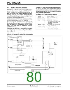
PIC17C75X
Example 10-7 shows the instruction sequence to initial-
ize PORTG. The Bank Select Register (BSR) must be
selected to Bank 5 for the port to be initialized. The fol-
lowing example uses the MOVLBinstruction to load the
BSR register for bank selection.
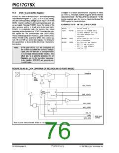
10.7
PORTG and DDRG Registers
PORTG is an 8-bit wide bi-directional port. The corre-
sponding data direction register is DDRG. A '1' in
DDRG configures the corresponding port pin as an
input. A '0' in the DDRG register configures the corre-
sponding port pin as an output. Reading PORTG
reads the status of the pins, whereas writing to them
will write to the respective port latch.
EXAMPLE 10-7: INITIALIZING PORTG
MOVLB
5
; Select Bank 5
MOVLW 0x0E
; Configure PORTG as
MOVPF ADCON1 ; digital
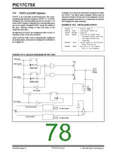
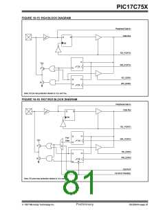
The lower four bits of PORTG are multiplexed with four
of the 12 channels of the 10-bit A/D converter.
CLRF
PORTG ; Initialize PORTG data
;
;
;
latches before setting
the data direction
register
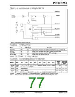
The remaining bits of PORTG are multiplexed with
peripheral output and inputs. RG4 is multiplexed with
the CAP3 input, RG5 is multiplexed with the PWM3
output, RG6 and RG7 are multiplexed with the
USART2 functions.
MOVLW
MOVWF
0x03 ; Value used to initialize
data direction
DDRG ; Set RG<1:0> as inputs
;
;
RG<7:2> as outputs
Upon reset the entire Port is automatically configured
as analog inputs, and must be configured in software
to be a digital I/O.
FIGURE 10-14: BLOCK DIAGRAM OF RG3:RG0
Data bus
D
Q
Q
VDD
P
WR PORTG
CK
Data Latch
I/O pin
D
Q
Q
N
WR DDRG
CK
VSS
DDRG Latch
ST
input
buffer
RD DDRG
Q
D
EN
EN
RD PORT
VAN
PCFG3:PCFG0
To other pads
To other pads
CHS3:CHS0
DS30264A-page 80
Preliminary
1997 Microchip Technology Inc.

 MICROCHIP [ MICROCHIP ]