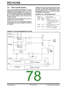
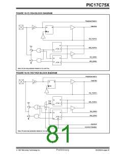
PIC17C75X
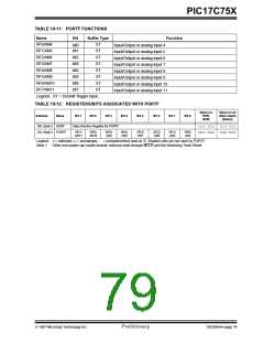
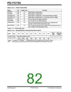
TABLE 10-13: PORTG FUNCTIONS
Name
Bit
Buffer Type
Function
RG0/AN3
ST
ST
ST
ST
ST
ST
ST
bit0
bit1
Input/Output or analog input 3.
Input/Output or analog input 2.
RG1/AN2
RG2/AN1/VREF-
RG3/AN0/VREF+
RG4/CAP3
RG5/PWM3
RG6/RX2/DT2
bit2
bit3
bit4
bit5
bit6
Input/Output or analog input 1 or the ground reference voltage
Input/Output or analog input 0 or the positive reference voltage
RG4 can also be the Capture3 input pin.
RG5 can also be the PWM3 output pin.
RG6 can also be selected as the USART2 (SCI) Asynchronous
Receive or USART2 (SCI) Synchronous Data.
RG7/TX2/CK2
bit7
ST
RG7 can also be selected as the USART2 (SCI) Asynchronous Trans-
mit or USART2 (SCI) Synchronous Clock.
Legend: ST = Schmitt Trigger input.
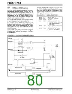
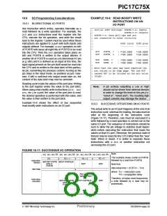
TABLE 10-14: REGISTERS/BITS ASSOCIATED WITH PORTG
Value on,
POR,
BOR
Value on all
other resets
(Note1)
Address
Name
Bit 7
Bit 6
Bit 5
Bit 4
Bit 3
Bit 2
Bit 1
Bit 0
12h, Bank 5 DDRG
13h, Bank 5 PORTG
Data Direction Register for PORTG
1111 1111
xxxx 0000
1111 1111
uuuu 0000
RG7/
RG6/
RG5/
RG4/
CAP3
RG3/
AN0
RG2/
AN1
RG1/
AN2
RG0/
AN3
TX2/CK2 RX2/DT2
PWM3
Legend: x= unknown, u= unchanged, - = unimplemented read as '0'. Shaded cells are not used by PORTG.
Note 1: Other (non power-up) resets include: external reset through MCLR and the Watchdog Timer Reset.
DS30264A-page 82
Preliminary
1997 Microchip Technology Inc.

 MICROCHIP [ MICROCHIP ]