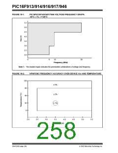
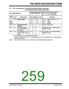
PIC16F913/914/916/917/946
19.0 ELECTRICAL SPECIFICATIONS
(†)
Absolute Maximum Ratings
Ambient temperature under bias..........................................................................................................-40° to +125°C
Storage temperature ........................................................................................................................ -65°C to +150°C
Voltage on VDD with respect to VSS ................................................................................................... -0.3V to +6.5V
Voltage on MCLR with respect to Vss ............................................................................................... -0.3V to +13.5V
Voltage on all other pins with respect to VSS ........................................................................... -0.3V to (VDD + 0.3V)
Total power dissipation(1) ...............................................................................................................................800 mW
Maximum current out of VSS pin ....................................................................................................................... 95 mA
Maximum current into VDD pin .......................................................................................................................... 95 mA
Input clamp current, IIK (VI < 0 or VI > VDD)................................................................................................................ 20 mA
Output clamp current, IOK (Vo < 0 or Vo >VDD).......................................................................................................... 20 mA
Maximum output current sunk by any I/O pin....................................................................................................25 mA
Maximum output current sourced by any I/O pin .............................................................................................. 25 mA
Maximum current sourced by all ports (combined) ........................................................................................... 90 mA
Maximum current sunk by all ports (combined) ................................................................................................ 90 mA
Note 1: Power dissipation is calculated as follows: PDIS = VDD x {IDD – ∑ IOH} + ∑ {(VDD – VOH) x IOH} + ∑(VOL x IOL).
2: PORTD and PORTE are not implemented in PIC16F913/916 devices.
† NOTICE: Stresses above those listed under “Absolute Maximum Ratings” may cause permanent damage to the
device. This is a stress rating only and functional operation of the device at those or any other conditions above those
indicated in the operation listings of this specification is not implied. Exposure to maximum rating conditions for
extended periods may affect device reliability.
© 2007 Microchip Technology Inc.
DS41250F-page 255

 MICROCHIP [ MICROCHIP ]