PIC16F913/914/916/917/946
16.9.1 ICD PINOUT
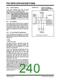
16.9 In-Circuit Debugger
The devices in the PIC16F91X/946 family carry the
circuitry for the In-Circuit Debugger on-chip and on
existing device pins. This eliminates the need for a
separate die or package for the ICD device. The
pinout for the ICD device is the same as the devices
(see Section 1.0 “Device Overview” for complete
pinout and pin descriptions). Table 16-9 shows the
location and function of the ICD related pins on the 28
and 40-pin devices.
When the debug bit in the Configuration Word register
is programmed to a ‘0’, the In-Circuit Debugger func-
tionality is enabled. This function allows simple debug-
ging functions when used with MPLAB® ICD 2. When
the microcontroller has this feature enabled, some of
the resources are not available for general use. See
Table 16-9 for more detail.
Note: The user’s application must have the
circuitry
required
to
support
ICD
functionality. Once the ICD circuitry is
enabled, normal device pin functions on
RB6/ICSPCLK/ICDCK/SEG14
and
RB7/ICSPDAT/ICDDAT/SEG13 will not be
usable. The ICD circuitry uses these pins for
communication with the ICD2 external
debugger.
For more information, see “Using MPLAB® ICD 2”
(DS51265), available on Microchip’s web site
(www.microchip.com).
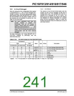
TABLE 16-9: PIC16F91X/946-ICD PIN DESCRIPTIONS
Pin Numbers
PDIP
TQFP
Name
Type Pull-up
Description
PIC16F914/917 PIC16F913/916
PIC16F946
40
39
28
27
1
24
ICDDATA
ICDCLK
TTL
ST
HV
P
—
—
—
—
—
—
—
In Circuit Debugger Bidirectional data
In Circuit Debugger Bidirectional clock
Programming voltage
Power
23
1
36
10, 19, 38, 51
9, 20, 41, 56
26
MCLR/VPP
VDD
11,32
12,31
—
20
8,19
—
VSS
P
Ground
AVDD
AVSS
P
Analog power
—
—
25
P
Analog ground
Legend:
TTL = TTL input buffer, ST = Schmitt Trigger input buffer, P = Power, HV = High Voltage
© 2007 Microchip Technology Inc.
DS41250F-page 239

 MICROCHIP [ MICROCHIP ]