PIC16F913/914/916/917/946
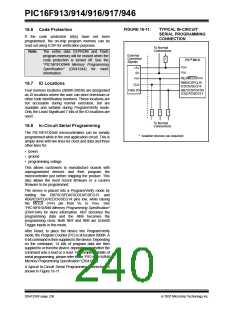
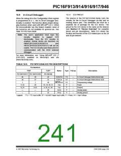
FIGURE 16-11:
TYPICAL IN-CIRCUIT
SERIAL PROGRAMMING
CONNECTION
16.6 Code Protection
If the code protection bit(s) have not been
programmed, the on-chip program memory can be
read out using ICSP for verification purposes.
To Normal
Connections
Note:
The entire data EEPROM and Flash
program memory will be erased when the
code protection is turned off. See the
“PIC16F91X/946 Memory Programming
Specification” (DS41244) for more
information.
External
Connector
Signals
PIC® MCU
*
VDD
+5V
0V
VSS
RE3/MCLR/VPP
VPP
RB6/ICSPCLK/
ICDCK/SEG14
RB7/ICSPDATA/
ICDDAT/SEG13
16.7 ID Locations
CLK
Data I/O
Four memory locations (2000h-2003h) are designated
as ID locations where the user can store checksum or
other code identification numbers. These locations are
not accessible during normal execution, but are
readable and writable during Program/Verify mode.
Only the Least Significant 7 bits of the ID locations are
used.
*
*
*
To Normal
Connections
16.8 In-Circuit Serial Programming
The PIC16F91X/946 microcontrollers can be serially
programmed while in the end application circuit. This is
simply done with two lines for clock and data and three
other lines for:
* Isolation devices (as required)
• power
• ground
• programming voltage
This allows customers to manufacture boards with
unprogrammed devices and then program the
microcontroller just before shipping the product. This
also allows the most recent firmware or a custom
firmware to be programmed.
The device is placed into a Program/Verify mode by
holding the RB7/ICSPDAT/ICDDAT/SEG13 and
RB6/ICSPCLK/ICDCK/SEG14 pins low, while raising
the MCLR (VPP) pin from VIL to VIHH. See
“PIC16F91X/946 Memory Programming Specification”
(DS41244) for more information. RB7 becomes the
programming data and the RB6 becomes the
programming clock. Both RB7 and RB6 are Schmitt
Trigger inputs in this mode.
After Reset, to place the device into Program/Verify
mode, the Program Counter (PC) is at location 0000h. A
6-bit command is then supplied to the device. Depending
on the command, 14 bits of program data are then
supplied to or from the device, depending on whether the
command was a load or a read. For complete details of
serial programming, please refer to the “PIC16F91X/946
Memory Programming Specification” (DS41244).
A typical In-Circuit Serial Programming connection is
shown in Figure 16-11.
DS41250F-page 238
© 2007 Microchip Technology Inc.

 MICROCHIP [ MICROCHIP ]