PIC16F913/914/916/917/946
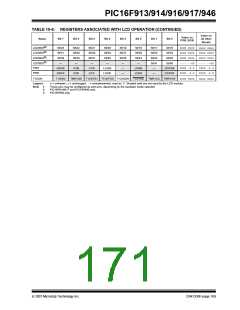
TABLE 10-6: REGISTERS ASSOCIATED WITH LCD OPERATION (CONTINUED)
Value on
all other
Resets
Value on
POR, BOR
Name
Bit 7
Bit 6
Bit 5
Bit 4
Bit 3
Bit 2
Bit 1
Bit 0
LCDSE2(2)
LCDSE3(3)
LCDSE4(3)
SE23
SE31
SE39
—
SE22
SE30
SE38
—
SE21
SE29
SE37
—
SE20
SE28
SE36
—
SE19
SE27
SE35
—
SE18
SE26
SE34
—
SE17
SE25
SE33
SE41
—
SE16
SE24
0000 0000
0000 0000
0000 0000
uuuu uuuu
0000 0000
0000 0000
SE32
LCDSE5(3)
PIE2
SE40
---- --00
0000 -0-0
0000 -0-0
---- --00
0000 -0-0
0000 -0-0
OSFIE
OSFIF
C2IE
C2IF
C1IE
C1IF
LCDIE
LCDIF
—
LVDIE
LVDIF
CCP2IE
CCP2IF
PIR2
—
—
T1CON
T1GINV
TMR1GE T1CKPS1 T1CKPS0 T1OSCEN T1SYNC
TMR1CS
TMR1ON
0000 0000
uuuu uuuu
Legend:
Note 1:
x= unknown, u= unchanged, -= unimplemented, read as ‘0’. Shaded cells are not used by the LCD module.
These pins may be configured as port pins, depending on the oscillator mode selected.
PIC16F914/917 and PIC16F946 only.
2:
3:
PIC16F946 only.
© 2007 Microchip Technology Inc.
DS41250F-page 169

 MICROCHIP [ MICROCHIP ]