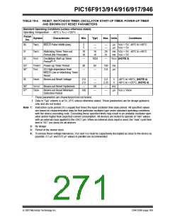
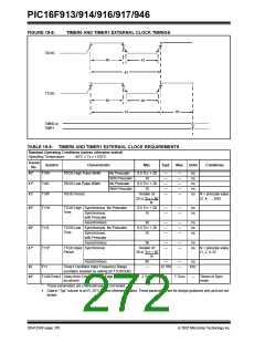
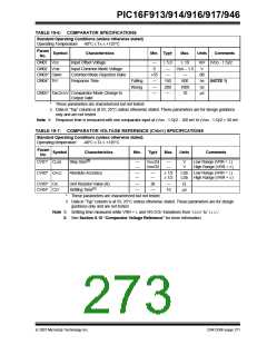
PIC16F913/914/916/917/946
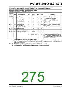
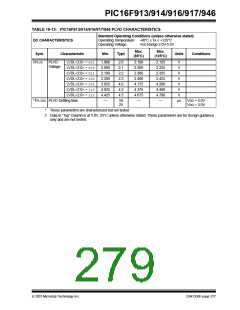
TABLE 19-9: PIC16F913/914/916/917/946 A/D CONVERSION REQUIREMENTS
Standard Operating Conditions (unless otherwise stated)
Operating temperature
-40°C ≤ TA ≤ +125°C
Param
No.
Sym.
Characteristic
A/D Clock Period
Min.
Typ†
Max. Units
Conditions
AD130* TAD
1.6
3.0
—
—
9.0
9.0
μs TOSC-based, VREF ≥ 3.0V
μs TOSC-based, VREF full range
A/D Internal RC
Oscillator Period
ADCS<1:0> = 11(ADRC mode)
μs At VDD = 2.5V
3.0
1.6
—
6.0
4.0
11
9.0
6.0
—
μs At VDD = 5.0V
AD131 TCNV Conversion Time
(not including
TAD Set GO/DONE bit to new data in A/D
Result register
Acquisition Time)(1)
AD132* TACQ Acquisition Time
11.5
—
—
5
μs
μs
—
AD133* TAMP Amplifier Settling Time
AD134 TGO Q4 to A/D Clock Start
—
—
TOSC/2
—
—
TOSC/2 + TCY
—
—
If the A/D clock source is selected as
RC, a time of TCY is added before the
A/D clock starts. This allows the SLEEP
instruction to be executed.
*
These parameters are characterized but not tested.
†
Data in “Typ” column is at 5.0V, 25°C unless otherwise stated. These parameters are for design guidance
only and are not tested.
Note 1: ADRESH and ADRESL registers may be read on the following TCY cycle.
2: See Section 12.3 “A/D Acquisition Requirements” for minimum conditions.
© 2007 Microchip Technology Inc.
DS41250F-page 273

 MICROCHIP [ MICROCHIP ]