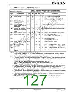
PIC16F872
14.1
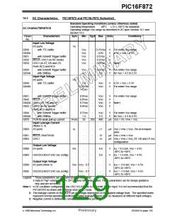
DC Characteristics:
PIC16F872 (Industrial)
Standard Operating Conditions (unless otherwise stated)
DC CHARACTERISTICS
Operating temperature
-40°C ≤ TA ≤ +85°C for industrial
Param
No.
Characteristic
Sym
Min Typ† Max Units
Conditions
D001 Supply Voltage
D001A
VDD
4.0
4.5
VBOR*
-
-
-
5.5
5.5
5.5
V
V
V
XT, RC and LP osc configuration
HS osc configuration
BOR enabled, Fmax = 14MHz (Note 7)
D002* RAM Data Retention
Voltage (Note 1)
VDR
-
-
1.5
-
V
D003
VDD start voltage to
ensure internal Power-on
Reset signal
VPOR
VSS
-
V
See section on Power-on Reset for details
D004* VDD rise rate to ensure
internal Power-on Reset
signal
SVDD
0.05
-
-
V/ms See section on Power-on Reset for details
D005 Brown-out Reset Voltage VBOR
3.7
-
4.0 4.35
V
BODEN bit in configuration word enabled
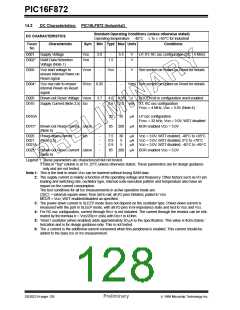
D010
D013
Supply Current (Note 2,5) IDD
1.6
4
mA XT, RC osc configuration
FOSC = 4 MHz, VDD = 5.5V (Note 4)
-
-
7
15
mA HS osc configuration
FOSC = 20 MHz, VDD = 5.5V
D015* Brown-out Reset Current ∆IBOR
85 200 µA BOR enabled VDD = 5.0V
(Note 6)
D020 Power-down Current
D021 (Note 3,5)
D021A
IPD
-
-
-
10.5 42 µA VDD = 4.0V, WDT enabled, -40°C to +85°C
1.5
1.5
16
19
µA VDD = 4.0V, WDT disabled, -0°C to +70°C
µA VDD = 4.0V, WDT disabled, -40°C to +85°C
D023* Brown-out Reset Current ∆IBOR
-
85 200 µA BOR enabled VDD = 5.0V
(Note 6)
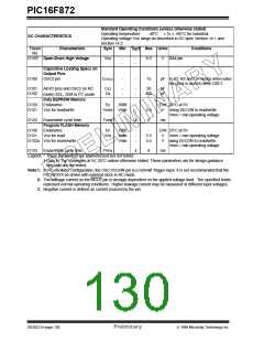
Legend: * These parameters are characterized but not tested.
† Data in "Typ" column is at 5V, 25°C unless otherwise stated. These parameters are for design guidance
only and are not tested.
Note 1: This is the limit to which VDD can be lowered without losing RAM data.
2: The supply current is mainly a function of the operating voltage and frequency. Other factors such as I/O pin
loading and switching rate, oscillator type, internal code execution pattern and temperature also have an
impact on the current consumption.
The test conditions for all IDD measurements in active operation mode are:
OSC1 = external square wave, from rail to rail; all I/O pins tristated, pulled to VDD
MCLR = VDD; WDT enabled/disabled as specified.
3: The power-down current in SLEEP mode does not depend on the oscillator type. Power-down current is mea-
sured with the part in SLEEP mode, with all I/O pins in hi-impedance state and tied to VDD and VSS.
4: For RC osc configuration, current through REXT is not included. The current through the resistor can be esti-
mated by the formula Ir = VDD/2REXT (mA) with REXT in kOhm.
5: Timer1 oscillator (when enabled) adds approximately 20 µA to the specification. This value is from character-
ization and is for design guidance only. This is not tested.
6: The ∆ current is the additional current consumed when this peripheral is enabled. This current should be
added to the base IDD or IPD measurement.
7: When BOR is enabled, the device will operate correctly until the VBOR voltage trip point is reached.
1999 Microchip Technology Inc.
Preliminary
DS30221A-page 127

 MICROCHIP [ MICROCHIP ]