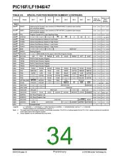
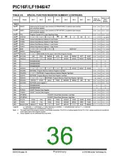
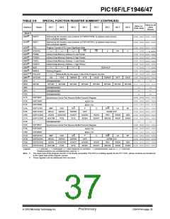
PIC16F/LF1946/47
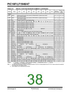
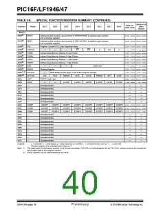
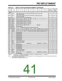
TABLE 3-9:
SPECIAL FUNCTION REGISTER SUMMARY (CONTINUED)
Value on all
other
Resets
Value on:
POR, BOR
Address
Name
Bit 7
Bit 6
Bit 5
Bit 4
Bit 3
Bit 2
Bit 1
Bit 0
Bank 5
280h(2)
INDF0
INDF1
Addressing this location uses contents of FSR0H/FSR0L to address data memory
(not a physical register)
xxxx xxxx xxxx xxxx
xxxx xxxx xxxx xxxx
281h(2)
Addressing this location uses contents of FSR1H/FSR1L to address data memory
(not a physical register)
282h(2)
283h(2)
284h(2)
285h(2)
286h(2)
287h(2)
288h(2)
289h(2)
PCL
Program Counter (PC) Least Significant Byte
0000 0000 0000 0000
---1 1000 ---q quuu
0000 0000 uuuu uuuu
0000 0000 0000 0000
0000 0000 uuuu uuuu
0000 0000 0000 0000
---0 0000 ---0 0000
0000 0000 uuuu uuuu
-000 0000 -000 0000
0000 000x 0000 000u
xxxx xxxx uuuu uuuu
--xx xxxx --uu uuuu
STATUS
FSR0L
FSR0H
FSR1L
FSR1H
BSR
—
—
—
TO
PD
Z
DC
C
Indirect Data Memory Address 0 Low Pointer
Indirect Data Memory Address 0 High Pointer
Indirect Data Memory Address 1 Low Pointer
Indirect Data Memory Address 1 High Pointer
—
—
—
BSR<4:0>
WREG
Working Register
28Ah(1, 2) PCLATH
—
Write Buffer for the upper 7 bits of the Program Counter
PEIE TMR0IE INTE IOCIE
28Bh(2)
28Ch
28Dh
28Eh
28Fh
290h
291h
292h
293h
294h
295h
296h
297h
298h
299h
29Ah
29Bh
29Ch
29Dh
29Eh
29Fh
Legend:
INTCON
PORTF
GIE
TMR0IF
INTF
RG1
IOCIF
RG0
PORTF Data Latch when written: PORTF pins when read
PORTG
—
—
—
RG5
RG4
RG3
RG2
Unimplemented
Unimplemented
Unimplemented
—
—
—
—
—
—
—
—
CCPR1L
CCPR1H
CCP1CON
PWM1CON
CCP1AS
PSTR1CON
—
Capture/Compare/PWM Register 1 (LSB)
Capture/Compare/PWM Register 1 (MSB)
xxxx xxxx uuuu uuuu
xxxx xxxx uuuu uuuu
0000 0000 0000 0000
0000 0000 0000 0000
0000 0000 0000 0000
P1M<1:0>
P1RSEN
DC1B<1:0>
CCP1M<3:0>
P1DC<6:0>
STR1D
CCP1ASE
—
CCP1AS<2:0>
—
PSS1AC<1:0>
PSS1BD<1:0>
STR1B STR1A ---0 0001 ---0 0001
—
STR1SYNC
STR1C
Unimplemented
—
—
CCPR2L
CCPR2H
CCP2CON
PWM2CON
CCP2AS
PSTR2CON
CCPTMRS0
CCPTMRS1
Capture/Compare/PWM Register 2 (LSB)
Capture/Compare/PWM Register 2 (MSB)
xxxx xxxx uuuu uuuu
xxxx xxxx uuuu uuuu
0000 0000 0000 0000
0000 0000 0000 0000
0000 0000 0000 0000
P2M<1:0>
P2RSEN
DC2B<1:0>
CCP2M<3:0>
P2DC<6:0>
CCP2ASE
—
CCP2AS<2:0>
PSS2AC<1:0>
STR2D STR2C
C2TSEL1 C2TSEL0 C1TSEL1 C1TSEL0 0000 0000 0000 0000
C5TSEL<1:0> ---- --00 ---- --00
PSS2BD<1:0>
—
—
C3TSEL1
—
STR2SYNC
C3TSEL0
—
STR2B
STR2A ---0 0001 ---0 0001
C4TSEL1 C4TSEL0
—
—
—
—
x= unknown, u= unchanged, q= value depends on condition, - = unimplemented, read as ‘0’, r= reserved.
Shaded locations are unimplemented, read as ‘0’.
Note 1: The upper byte of the program counter is not directly accessible. PCLATH is a holding register for the PC<14:8>, whose contents are transferred
to the upper byte of the program counter.
2: These registers can be addressed from any bank.
DS41414A-page 36
Preliminary
2010 Microchip Technology Inc.

 MICROCHIP [ MICROCHIP ]