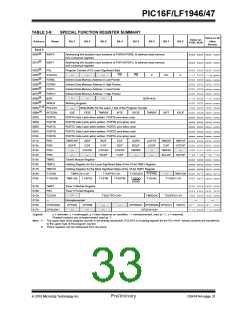
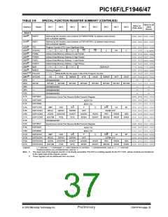
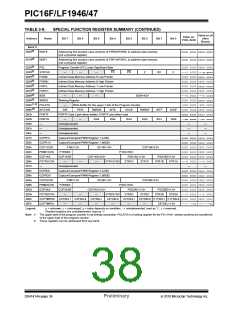
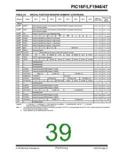
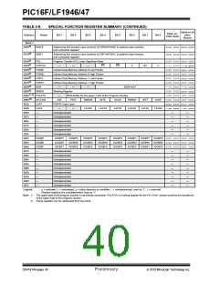
PIC16F/LF1946/47
TABLE 3-9:
SPECIAL FUNCTION REGISTER SUMMARY (CONTINUED)
Value on all
other
Resets
Value on:
POR, BOR
Address
Name
Bit 7
Bit 6
Bit 5
Bit 4
Bit 3
Bit 2
Bit 1
Bit 0
Bank 4
200h(2)
INDF0
INDF1
Addressing this location uses contents of FSR0H/FSR0L to address data memory
(not a physical register)
xxxx xxxx xxxx xxxx
xxxx xxxx xxxx xxxx
201h(2)
Addressing this location uses contents of FSR1H/FSR1L to address data memory
(not a physical register)
202h(2)
203h(2)
204h(2)
205h(2)
206h(2)
207h(2)
208h(2)
209h(2)
PCL
Program Counter (PC) Least Significant Byte
0000 0000 0000 0000
---1 1000 ---q quuu
0000 0000 uuuu uuuu
0000 0000 0000 0000
0000 0000 uuuu uuuu
0000 0000 0000 0000
---0 0000 ---0 0000
0000 0000 uuuu uuuu
-000 0000 -000 0000
0000 000x 0000 000u
STATUS
FSR0L
FSR0H
FSR1L
FSR1H
BSR
—
—
—
TO
PD
Z
DC
C
Indirect Data Memory Address 0 Low Pointer
Indirect Data Memory Address 0 High Pointer
Indirect Data Memory Address 1 Low Pointer
Indirect Data Memory Address 1 High Pointer
—
—
—
BSR<4:0>
WREG
Working Register
20Ah(1, 2) PCLATH
—
Write Buffer for the upper 7 bits of the Program Counter
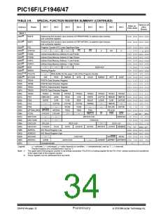
20Bh(2)
20Ch
20Dh
20Eh
20Fh
210h
211h
INTCON
—
GIE
PEIE
TMR0IE
INTE
IOCIE
TMR0IF
INTF
IOCIF
Unimplemented
—
—
WPUB
—
WPUB7
WPUB6
WPUB5
WPUB4
WPUB3
WPUB2
WPUB1
WPUB0 1111 1111 1111 1111
Unimplemented
Unimplemented
Unimplemented
—
—
—
—
—
—
—
—
SSP1BUF
SSP1ADD
SSP1MSK
xxxx xxxx uuuu uuuu
0000 0000 0000 0000
1111 1111 1111 1111
Synchronous Serial Port Receive Buffer/Transmit Register
212h
213h
ADD<7:0>
MSK<7:0>
214h
215h
216h
217h
218h
219h
21Ah
21Bh
SSP1STAT
SSP1CON1
SSP1CON2
SSP1CON3
—
SMP
WCOL
GCEN
ACKTIM
CKE
SSPOV
ACKSTAT
PCIE
D/A
P
S
R/W
UA
BF
0000 0000 0000 0000
0000 0000 0000 0000
0000 0000 0000 0000
0000 0000 0000 0000
SSPEN
ACKDT
SCIE
CKP
SSPM<3:0>
ACKEN
BOEN
RCEN
PEN
RSEN
AHEN
SEN
SDAHT
SBCDE
DHEN
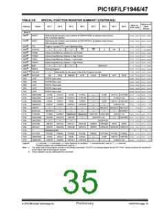
Unimplemented
—
—
SSP2BUF
SSP2ADD
SSP2MSK
xxxx xxxx uuuu uuuu
0000 0000 0000 0000
1111 1111 1111 1111
Synchronous Serial Port Receive Buffer/Transmit Register
ADD<7:0>
MSK<7:0>
21Ch
SSP2STAT
SSP2CON1
SSP2CON2
SSP2CON3
SMP
WCOL
GCEN
ACKTIM
CKE
SSPOV
ACKSTAT
PCIE
D/A
P
S
R/W
UA
BF
0000 0000 0000 0000
0000 0000 0000 0000
0000 0000 0000 0000
0000 0000 0000 0000
21Dh
SSPEN
ACKDT
SCIE
CKP
SSPM<3:0>
21Eh
ACKEN
BOEN
RCEN
PEN
RSEN
AHEN
SEN
21Fh
SDAHT
SBCDE
DHEN
Legend:
x= unknown, u= unchanged, q= value depends on condition, - = unimplemented, read as ‘0’, r= reserved.
Shaded locations are unimplemented, read as ‘0’.
Note 1: The upper byte of the program counter is not directly accessible. PCLATH is a holding register for the PC<14:8>, whose contents are transferred
to the upper byte of the program counter.
2: These registers can be addressed from any bank.
2010 Microchip Technology Inc.
Preliminary
DS41414A-page 35

 MICROCHIP [ MICROCHIP ]