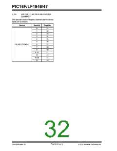
PIC16F/LF1946/47
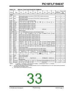
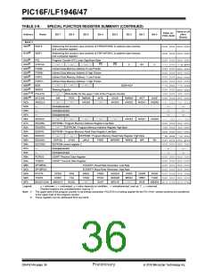
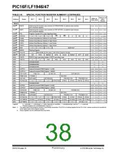
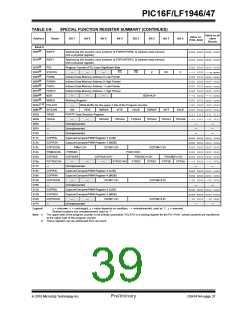
TABLE 3-9:
SPECIAL FUNCTION REGISTER SUMMARY (CONTINUED)
Value on all
other
Resets
Value on:
POR, BOR
Address
Name
Bit 7
Bit 6
Bit 5
Bit 4
Bit 3
Bit 2
Bit 1
Bit 0
Bank 3
180h(2)
INDF0
INDF1
Addressing this location uses contents of FSR0H/FSR0L to address data memory
(not a physical register)
xxxx xxxx xxxx xxxx
xxxx xxxx xxxx xxxx
181h(2)
Addressing this location uses contents of FSR1H/FSR1L to address data memory
(not a physical register)
182h(2)
183h(2)
184h(2)
185h(2)
186h(2)
187h(2)
188h(2)
189h(2)
PCL
Program Counter (PC) Least Significant Byte
0000 0000 0000 0000
---1 1000 ---q quuu
0000 0000 uuuu uuuu
0000 0000 0000 0000
0000 0000 uuuu uuuu
0000 0000 0000 0000
---0 0000 ---0 0000
0000 0000 uuuu uuuu
-000 0000 -000 0000
0000 000x 0000 000u
STATUS
FSR0L
FSR0H
FSR1L
FSR1H
BSR
—
—
—
TO
PD
Z
DC
C
Indirect Data Memory Address 0 Low Pointer
Indirect Data Memory Address 0 High Pointer
Indirect Data Memory Address 1 Low Pointer
Indirect Data Memory Address 1 High Pointer
—
—
—
BSR<4:0>
WREG
Working Register
18Ah(1, 2) PCLATH
—
GIE
—
Write Buffer for the upper 7 bits of the Program Counter
18Bh(2)
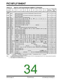
18Ch
18Dh
18Eh
18Fh
190h
191h
192h
193h
194h
195h
196h
197h
198h
199h
19Ah
19Bh
19Ch
19Dh
19Eh
19Fh
Legend:
INTCON
ANSELA
—
PEIE
—
TMR0IE
ANSA5
INTE
—
IOCIE
TMR0IF
ANSA2
INTF
IOCIF
ANSA3
ANSA1
ANSA0 --1- 1111 --1- 1111
Unimplemented
Unimplemented
Unimplemented
—
—
—
—
—
—
—
—
—
ANSELE
EEADRL
EEADRH
EEDATL
EEDATH
EECON1
EECON2
—
—
—
—
—
ANSE2
ANSE1
ANSE0 ---- -111 ---- -111
0000 0000 0000 0000
-000 0000 -000 0000
xxxx xxxx uuuu uuuu
--xx xxxx --uu uuuu
EEPROM / Program Memory Address Register Low Byte
EEPROM / Program Memory Address Register High Byte
EEPROM / Program Memory Read Data Register Low Byte
—
—
—
EEPROM / Program Memory Read Data Register High Byte
EEPGD
CFGS
LWLO
FREE
WRERR
WREN
WR
RD
0000 x000 0000 q000
0000 0000 0000 0000
EEPROM control register 2
Unimplemented
—
—
—
—
—
Unimplemented
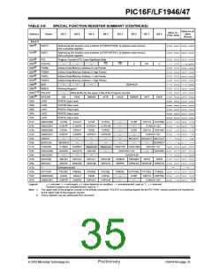
RCREG
TXREG
SP1BRGL
SP1BRGH
RCSTA
TXSTA
BAUD1CON
USART Receive Data Register
USART Transmit Data Register
0000 0000 0000 0000
0000 0000 0000 0000
0000 0000 0000 0000
0000 0000 0000 0000
0000 000x 0000 000x
0000 0010 0000 0010
EUSART1 Baud Rate Generator, Low Byte
EUSART1 Baud Rate Generator, High Byte
SPEN
CSRC
RX9
TX9
SREN
TXEN
—
CREN
SYNC
SCKP
ADDEN
SENDB
BRG16
FERR
BRGH
—
OERR
TRMT
WUE
RX9D
TX9D
ABDOVF
RCIDL
ABDEN 01-0 0-00 01-0 0-00
x= unknown, u= unchanged, q= value depends on condition, - = unimplemented, read as ‘0’, r= reserved.
Shaded locations are unimplemented, read as ‘0’.
Note 1: The upper byte of the program counter is not directly accessible. PCLATH is a holding register for the PC<14:8>, whose contents are transferred
to the upper byte of the program counter.
2: These registers can be addressed from any bank.
DS41414A-page 34
Preliminary
2010 Microchip Technology Inc.

 MICROCHIP [ MICROCHIP ]