PIC16F/LF1946/47
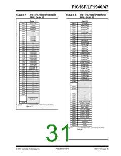
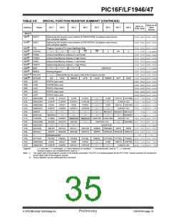
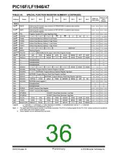
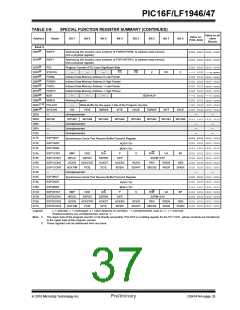
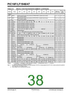
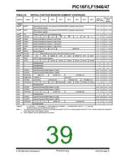
TABLE 3-9:
SPECIAL FUNCTION REGISTER SUMMARY (CONTINUED)
Value on all
other
Resets
Value on:
POR, BOR
Address
Name
Bit 7
Bit 6
Bit 5
Bit 4
Bit 3
Bit 2
Bit 1
Bit 0
Bank 2
100h(2)
INDF0
INDF1
Addressing this location uses contents of FSR0H/FSR0L to address data memory
(not a physical register)
xxxx xxxx xxxx xxxx
xxxx xxxx xxxx xxxx
101h(2)
Addressing this location uses contents of FSR1H/FSR1L to address data memory
(not a physical register)
102h(2)
103h(2)
104h(2)
105h(2)
106h(2)
107h(2)
108h(2)
109h(2)
PCL
Program Counter (PC) Least Significant Byte
0000 0000 0000 0000
---1 1000 ---q quuu
0000 0000 uuuu uuuu
0000 0000 0000 0000
0000 0000 uuuu uuuu
0000 0000 0000 0000
---0 0000 ---0 0000
0000 0000 uuuu uuuu
-000 0000 -000 0000
0000 000x 0000 000u
xxxx xxxx uuuu uuuu
xxxx xxxx uuuu uuuu
xxxx xxxx uuuu uuuu
xxxx xxxx uuuu uuuu
xxxx xxxx uuuu uuuu
STATUS
FSR0L
FSR0H
FSR1L
FSR1H
BSR
—
—
—
TO
PD
Z
DC
C
Indirect Data Memory Address 0 Low Pointer
Indirect Data Memory Address 0 High Pointer
Indirect Data Memory Address 1 Low Pointer
Indirect Data Memory Address 1 High Pointer
—
—
—
BSR<4:0>
WREG
Working Register
10Ah(1, 2) PCLATH
—
Write Buffer for the upper 7 bits of the Program Counter
10Bh(2)
10Ch
10Dh
10Eh
10Fh
110h
111h
INTCON
LATA
GIE
PEIE
TMR0IE
INTE
IOCIE
TMR0IF
INTF
IOCIF
PORTA Data Latch
PORTB Data Latch
PORTC Data Latch
PORTD Data Latch
PORTE Data Latch
LATB
LATC
LATD
LATE
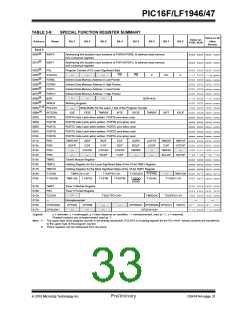
CM1CON0
CM1CON1
CM2CON0
CM2CON1
CMOUT
BORCON
FVRCON
DACCON0
DACCON1
SRCON0
SRCON1
—
C1ON
C1INTP
C2ON
C2INTP
—
C1OUT
C1OE
C1PCH1
C2OE
C2PCH1
—
C1POL
C1PCH0
C2POL
C2PCH0
—
—
—
—
—
—
—
C1SP
—
C1HYS C1SYNC 0000 -100 0000 -100
C1NCH<1:0> 0000 --00 0000 --00
C2HYS C2SYNC 0000 -100 0000 -100
C2NCH<1:0> 0000 --00 0000 --00
112h
113h
114h
115h
116h
117h
118h
119h
11Ah
11Bh
11Ch
11Dh
11Eh
11Fh
Legend:
C1INTN
C2OUT
C2INTN
—
C2SP
—
MC3OUT MC2OUT MC1OUT ---- -000 ---- -000
BORRDY 1--- ---q u--- ---u
ADFVR<1:0> 0q00 0000 0q00 0000
SBOREN
FVREN
DACEN
—
—
—
—
—
—
FVRRDY
DACLPS
—
Reserved
DACOE
—
Reserved CDAFVR1 CDAFVR0
—
DACPSS<1:0>
DACR<4:0>
SRNQEN
—
DACNSS 000- 00-0 000- 00-0
---0 0000 ---0 0000
SRLEN
SRSPE
SRCLK2
SRSCKE
SRCLK1
SRSC2E
SRCLK0
SRSC1E
SRQEN
SRRPE
SRPS
SRPR
0000 0000 0000 0000
SRRCKE SRRC2E SRRC1E 0000 0000 0000 0000
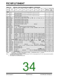
Unimplemented
—
—
APFCON
CM3CON0
CM3CON1
P3CSEL
C3ON
P3BSEL
P2DSEL
C3OE
P2CSEL
C3POL
P2BSEL
CCP2SEL P1CSEL P1BSEL 0000 0000 0000 0000
C3OUT
C3INTN
—
—
C3SP
—
C3HYS C3SYNC 0000 -100 0000 -100
C3NCH<1:0> 0000 --00 0000 --00
C3INTP
C3PCH1
C3PCH0
x= unknown, u= unchanged, q= value depends on condition, - = unimplemented, read as ‘0’, r= reserved.
Shaded locations are unimplemented, read as ‘0’.
Note 1: The upper byte of the program counter is not directly accessible. PCLATH is a holding register for the PC<14:8>, whose contents are transferred
to the upper byte of the program counter.
2: These registers can be addressed from any bank.
2010 Microchip Technology Inc.
Preliminary
DS41414A-page 33

 MICROCHIP [ MICROCHIP ]