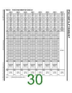
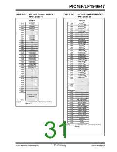
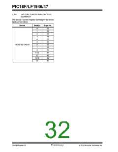
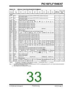
PIC16F/LF1946/47
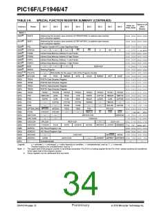
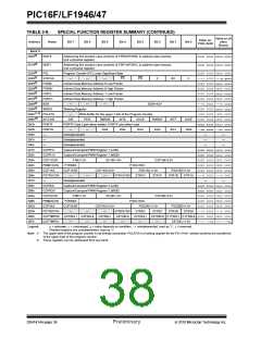
TABLE 3-9:
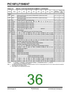
SPECIAL FUNCTION REGISTER SUMMARY (CONTINUED)
Value on all
other
Resets
Value on:
POR, BOR
Address
Name
Bit 7
Bit 6
Bit 5
Bit 4
Bit 3
Bit 2
Bit 1
Bit 0
Bank 1
080h(2)
INDF0
INDF1
Addressing this location uses contents of FSR0H/FSR0L to address data memory
(not a physical register)
xxxx xxxx xxxx xxxx
xxxx xxxx xxxx xxxx
081h(2)
Addressing this location uses contents of FSR1H/FSR1L to address data memory
(not a physical register)
082h(2)
083h(2)
084h(2)
085h(2)
086h(2)
087h(2)
088h(2)
089h(2)
PCL
Program Counter (PC) Least Significant Byte
0000 0000 0000 0000
---1 1000 ---q quuu
0000 0000 uuuu uuuu
0000 0000 0000 0000
0000 0000 uuuu uuuu
0000 0000 0000 0000
---0 0000 ---0 0000
0000 0000 uuuu uuuu
-000 0000 -000 0000
0000 000x 0000 000u
1111 1111 1111 1111
1111 1111 1111 1111
1111 1111 1111 1111
1111 1111 1111 1111
STATUS
FSR0L
FSR0H
FSR1L
FSR1H
BSR
—
—
—
TO
PD
Z
DC
C
Indirect Data Memory Address 0 Low Pointer
Indirect Data Memory Address 0 High Pointer
Indirect Data Memory Address 1 Low Pointer
Indirect Data Memory Address 1 High Pointer
—
—
—
BSR<4:0>
WREG
Working Register
08Ah(1, 2) PCLATH
—
Write Buffer for the upper 7 bits of the Program Counter
08Bh(2)
08Ch
08Dh
08Eh
08Fh
090h
091h
092h
093h
094h
095h
096h
097h
098h
099h
09Ah
09Bh
09Ch
09Dh
09Eh
09Fh
Legend:
INTCON
TRISA
TRISB
TRISC
TRISD
TRISE
PIE1
GIE
PEIE
TMR0IE
INTE
IOCIE
TMR0IF
INTF
IOCIF
PORTA Data Direction Register
PORTB Data Direction Register
PORTC Data Direction Register
PORTD Data Direction Register
TRISE7
TMR1GIE
OSFIE
—
TRISE6
ADIE
C2IE
TRISE5
RCIE
C1IE
TRISE4
TXIE
TRISE3
SSPIE
TRISE2
CCP1IE
LCDIE
—
TRISE1
TMR2IE
C3IE
TRISE0 1111 1111 1111 1111
TMR1IE 0000 0000 0000 0000
CCP2IE 0000 0000 0000 0000
PIE2
EEIE
BCLIE
PIE3
CCP5IE
—
CCP4IE
RC2IE
T0CS
—
CCP3IE
TX2IE
T0SE
—
TMR6IE
—
TMR4IE
BCL2IE
PS<2:0>
POR
—
-000 0-0- -000 0-0-
PIE4
—
—
SSP2IE --00 --00 --00 --00
OPTION_REG WPUEN
INTEDG
STKUNF
—
PSA
1111 1111 1111 1111
PCON
STKOVF
—
RMCLR
WDTPS<4:0>
RI
BOR
00-- 11qq qq-- qquu
WDTCON
OSCTUNE
OSCCON
OSCSTAT
ADRESL
ADRESH
ADCON0
ADCON1
—
SWDTEN --01 0110 --01 0110
—
—
TUN<5:0>
--00 0000 --00 0000
SPLLEN
T1OSCR
IRCF<3:0>
—
SCS<1:0>
0011 1-00 0011 1-00
HFIOFS 00q0 0q0- qqqq qq0-
xxxx xxxx uuuu uuuu
PLLR
OSTS
HFIOFR
HFIOFL
MFIOFR
LFIOFR
A/D Result Register Low
A/D Result Register High
—
xxxx xxxx uuuu uuuu
CHS<4:0>
GO/DONE
ADON
-000 0000 -000 0000
ADFM
ADCS<2:0>
—
ADNREF ADPREF1 ADPREF0 0000 -000 0000 -000
Unimplemented
—
—
x= unknown, u= unchanged, q= value depends on condition, - = unimplemented, read as ‘0’, r= reserved.
Shaded locations are unimplemented, read as ‘0’.
Note 1: The upper byte of the program counter is not directly accessible. PCLATH is a holding register for the PC<14:8>, whose contents are transferred
to the upper byte of the program counter.
2: These registers can be addressed from any bank.
DS41414A-page 32
Preliminary
2010 Microchip Technology Inc.

 MICROCHIP [ MICROCHIP ]