PIC16F/LF1946/47
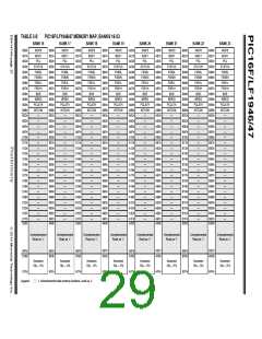
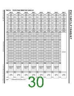
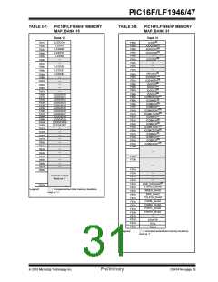
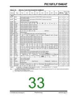
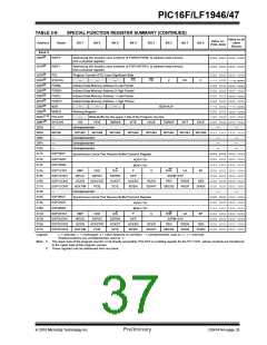
TABLE 3-9:
SPECIAL FUNCTION REGISTER SUMMARY
Value on all
other
Resets
Value on:
POR, BOR
Address
Name
Bit 7
Bit 6
Bit 5
Bit 4
Bit 3
Bit 2
Bit 1
Bit 0
Bank 0
000h(2)
INDF0
INDF1
Addressing this location uses contents of FSR0H/FSR0L to address data memory
(not a physical register)
xxxx xxxx xxxx xxxx
xxxx xxxx xxxx xxxx
001h(2)
Addressing this location uses contents of FSR1H/FSR1L to address data memory
(not a physical register)
002h(2)
003h(2)
004h(2)
005h(2)
006h(2)
007h(2)
008h(2)
009h(2)
PCL
Program Counter (PC) Least Significant Byte
0000 0000 0000 0000
---1 1000 ---q quuu
0000 0000 uuuu uuuu
0000 0000 0000 0000
0000 0000 uuuu uuuu
0000 0000 0000 0000
---0 0000 ---0 0000
0000 0000 uuuu uuuu
-000 0000 -000 0000
0000 000x 0000 000u
xxxx xxxx uuuu uuuu
xxxx xxxx uuuu uuuu
xxxx xxxx uuuu uuuu
xxxx xxxx uuuu uuuu
xxxx xxxx xxxx uuuu
STATUS
FSR0L
FSR0H
FSR1L
FSR1H
BSR
—
—
—
TO
PD
Z
DC
C
Indirect Data Memory Address 0 Low Pointer
Indirect Data Memory Address 0 High Pointer
Indirect Data Memory Address 1 Low Pointer
Indirect Data Memory Address 1 High Pointer
—
—
—
BSR<4:0>
WREG
Working Register
00Ah(1, 2) PCLATH
—
Write Buffer for the upper 7 bits of the Program Counter
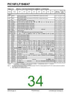
00Bh(2)
00Ch
00Dh
00Eh
00Fh
010h
011h
012h
013h
014h
015h
016h
017h
018h
019h
INTCON
PORTA
PORTB
PORTC
PORTD
PORTE
PIR1
GIE
PEIE
TMR0IE
INTE
IOCIE
TMR0IF
INTF
IOCIF
PORTA Data Latch when written: PORTA pins when read
PORTB Data Latch when written: PORTB pins when read
PORTC Data Latch when written: PORTC pins when read
PORTD Data Latch when written: PORTD pins when read
PORTE Data Latch when written: PORTE pins when read
TMR1GIF
OSFIF
—
ADIF
C2IF
RCIF
C1IF
TXIF
EEIF
SSPIF
BCLIF
TMR6IF
—
CCP1IF
LCDIF
—
TMR2IF
C3IF
TMR1IF 0000 0000 0000 0000
CCP2IF 0000 0000 0000 0000
PIR2
PIR3
CCP5IF
—
CCP4IF
RC2IF
CCP3IF
TX2IF
TMR4IF
BCL2IF
—
-000 0-0- -000 0-0-
PIR4
—
—
SSP2IF --00 --00 --00 --00
xxxx xxxx uuuu uuuu
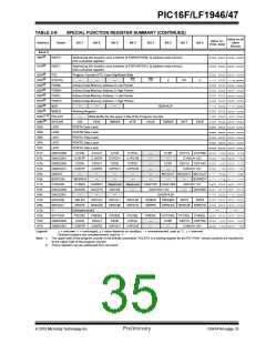
TMR0
Timer0 Module Register
TMR1L
TMR1H
T1CON
T1GCON
Holding Register for the Least Significant Byte of the 16-bit TMR1 Register
Holding Register for the Most Significant Byte of the 16-bit TMR1 Register
xxxx xxxx uuuu uuuu
xxxx xxxx uuuu uuuu
TMR1CS<1:0>
TMR1GE T1GPOL
T1CKPS<1:0>
T1GTM T1GSPM
T1OSCEN T1SYNC
—
TMR1ON 0000 00-0 uuuu uu-u
T1GGO/
DONE
T1GVAL
T1GSS<1:0>
0000 0x00 uuuu uxuu
01Ah
TMR2
Timer 2 Module Register
Timer 2 Period Register
—
0000 0000 0000 0000
1111 1111 1111 1111
-000 0000 -000 0000
01Bh
01Ch
01Dh
01Eh
01Fh
PR2
T2CON
—
T2OUTPS<3:0>
TMR2ON
T2CKPS<1:0>
Unimplemented
—
—
CPSCON0
CPSCON1
CPSON
—
CPSRM
—
—
—
—
CPSRNG1 CPSRNG0 CPSOUT T0XCS 00-- 0000 00-- 0000
CPSCH<4:0> ---0 0000 ---0 0000
Legend:
x= unknown, u= unchanged, q= value depends on condition, - = unimplemented, read as ‘0’, r= reserved.
Shaded locations are unimplemented, read as ‘0’.
Note 1: The upper byte of the program counter is not directly accessible. PCLATH is a holding register for the PC<14:8>, whose contents are transferred
to the upper byte of the program counter.
2: These registers can be addressed from any bank.
2010 Microchip Technology Inc.
Preliminary
DS41414A-page 31

 MICROCHIP [ MICROCHIP ]