PIC16F/LF1946/47
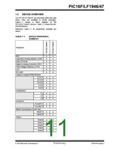
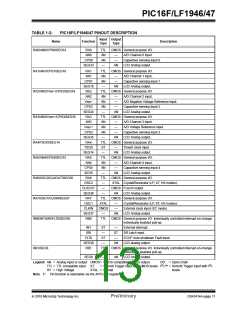
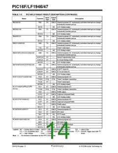
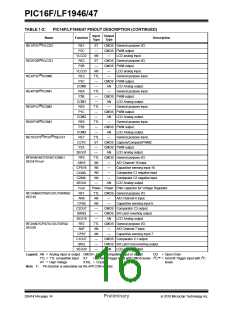
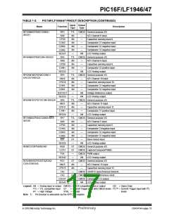
TABLE 1-2:
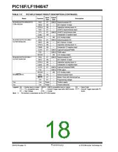
PIC16F/LF1946/47 PINOUT DESCRIPTION (CONTINUED)
Input Output
Name
Function
Description
Type
Type
RB2/SEG9
RB2
TTL
CMOS General purpose I/O. Individually controlled interrupt-on-change.
Individually enabled pull-up.
SEG9
RB3
—
AN
LCD Analog output.
RB3/SEG10
RB4/SEG11
RB5/T1G/SEG29
TTL
CMOS General purpose I/O. Individually controlled interrupt-on-change.
Individually enabled pull-up.
SEG10
RB4
—
AN
LCD Analog output.
TTL
CMOS General purpose I/O. Individually controlled interrupt-on-change.
Individually enabled pull-up.
SEG11
RB5
—
AN
LCD Analog output.
TTL
CMOS General purpose I/O. Individually controlled interrupt-on-change.
Individually enabled pull-up.
T1G
SEG29
RB6
ST
—
—
Timer1 Gate input.
LCD Analog output.
AN
RB6/ICSPCLK/ICDCLK/SEG38
RB7/ICSPDAT/ICDDAT/SEG39
RC0/T1OSO/T1CKI/SEG40
TTL
CMOS General purpose I/O. Individually controlled interrupt-on-change.
Individually enabled pull-up.
ICSPCLK
ICDCLK
SEG38
RB7
ST
ST
—
—
—
Serial Programming Clock.
In-Circuit Debug Clock.
LCD Analog output.
AN
TTL
CMOS General purpose I/O. Individually controlled interrupt-on-change.
Individually enabled pull-up.
ICSPDAT
ICDDAT
SEG39
RC0
ST
ST
—
CMOS ICSP™ Data I/O.
CMOS In-Circuit Data I/O.
AN
LCD Analog output.
ST
XTAL
ST
—
CMOS General purpose I/O.
T1OSO
T1CKI
SEG40
RC1
XTAL Timer1 oscillator connection.
—
Timer1 clock input.
LCD Analog output.
AN
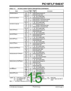
(1)
(1)
RC1/T1OSI/P2A /CCP2
/
ST
XTAL
—
CMOS General purpose I/O.
XTAL Timer1 oscillator connection.
CMOS PWM output.
SEG32
T1OSI
P2A
CCP2
SEG32
RC2
ST
—
CMOS Capture/Compare/PWM2.
AN
LCD Analog output.
RC2/CCP1/P1A/SEG13
RC3/SCK/SCL/SEG17
RC4/SDI1/SDA1/SEG16
ST
ST
—
CMOS General purpose I/O.
CMOS Capture/Compare/PWM1.
CMOS PWM output.
CCP1
P1A
SEG13
RC3
—
AN
LCD Analog output.
ST
ST
CMOS General purpose I/O.
SCK
CMOS SPI clock.
2
2
SCL
I C
OD
AN
I C™ clock.
SEG17
RC4
—
ST
ST
LCD Analog output.
CMOS General purpose I/O.
SDI1
—
SPI data input.
2
2
SDA1
SEG16
I C
OD
AN
I C™ data input/output.
—
LCD Analog output.
Legend: AN = Analog input or output CMOS= CMOS compatible input or output
OD = Open Drain
2
2
TTL = TTL compatible input ST
HV = High Voltage
= Schmitt Trigger input with CMOS levels I C™ = Schmitt Trigger input with I C
levels
XTAL = Crystal
Note 1: Pin function is selectable via the APFCON register.
DS41414A-page 12
Preliminary
2010 Microchip Technology Inc.

 MICROCHIP [ MICROCHIP ]