PIC16C63A/65B/73B/74B
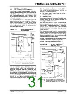
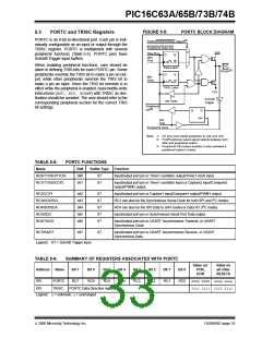
FIGURE 5-5:
PORTC BLOCK DIAGRAM
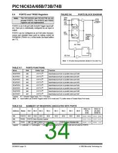
5.3
PORTC and TRISC Registers
PORTC is an 8-bit bi-directional port. Each pin is indi-
vidually configurable as an input or output through the
TRISC register. PORTC is multiplexed with several
peripheral functions (Table 5-5). PORTC pins have
Schmitt Trigger input buffers.
PORT/PERIPHERAL Select(2)
Peripheral Data Out
0
VDD
Data Bus
D
Q
Q
WR
P
Port
CK
1
When enabling peripheral functions, care should be
taken in defining TRIS bits for each PORTC pin. Some
peripherals override the TRIS bit to make a pin an out-
put, while other peripherals override the TRIS bit to
make a pin an input. Since the TRIS bit override is in
effect while the peripheral is enabled, read-modify-write
instructions (BSF, BCF, XORWF) with TRISC as des-
tination should be avoided. The user should refer to the
corresponding peripheral section for the correct TRIS
bit settings.
Data Latch
I/O pin(1)
D
Q
Q
WR
TRIS
CK
N
TRIS Latch
VSS
Schmitt
Trigger
RD TRIS
Peripheral
OE(3)
Q
D
EN
RD
Port
Peripheral Input
Note 1: I/O pins have diode protection to VDD and VSS.
2: Port/Peripheral select signal selects between port
data and peripheral output.
3: Peripheral OE (output enable) is only activated if
peripheral select is active.
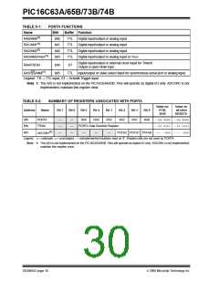
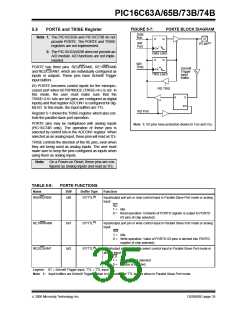
TABLE 5-5:
Name
PORTC FUNCTIONS
Bit#
bit0
bit1
Buffer Type
Function
RC0/T1OSO/T1CKI
RC1/T1OSI/CCP2
ST
ST
Input/output port pin or Timer1 oscillator output/Timer1 clock input.
Input/output port pin or Timer1 oscillator input or Capture2 input/Compare2
output/PWM2 output.
RC2/CCP1
bit2
bit3
bit4
bit5
bit6
ST
ST
ST
ST
ST
Input/output port pin or Capture1 input/Compare1 output/PWM1 output.
2
RC3/SCK/SCL
RC4/SDI/SDA
RC5/SDO
RC3 can also be the Synchronous Serial Clock for both SPI and I C modes.
2
RC4 can also be the SPI Data In (SPI mode) or Data I/O (I C mode).
Input/output port pin or Synchronous Serial Port Data output.
RC6/TX/CK
Input/output port pin or USART Asynchronous Transmit, or USART
Synchronous Clock.
RC7/RX/DT
bit7
ST
Input/output port pin or USART Asynchronous Receive, or USART
Synchronous Data.
Legend: ST = Schmitt Trigger input
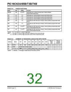
TABLE 5-6:
SUMMARY OF REGISTERS ASSOCIATED WITH PORTC
Value on:
POR,
BOR
Value on
all other
RESETS
Address
Name
Bit 7
Bit 6
Bit 5
Bit 4
Bit 3
Bit 2
Bit 1
Bit 0
07h
87h
PORTC
TRISC
RC7
RC6
RC5
RC4
RC3
RC2
RC1
RC0
xxxx xxxx
1111 1111
uuuu uuuu
1111 1111
PORTC Data Direction register
Legend: x= unknown, u= unchanged
2000 Microchip Technology Inc.
DS30605C-page 33

 MICROCHIP [ MICROCHIP ]